Preparation method of FS-IGBT (Field Stop-Insulated Gate Bipolar Translator)

A silicon wafer and backside technology, applied in the field of power semiconductor devices, can solve the problems of silicon wafer warpage, high difficulty, low yield rate, etc., and achieve the effect of reduced forward conduction voltage, small turn-off loss, and low yield rate

Active Publication Date: 2015-06-03
苏州翠展微电子有限公司
View PDF4 Cites 7 Cited by
  • Summary
  • Abstract
  • Description
  • Claims
  • Application Information

AI Technical Summary

Problems solved by technology

[0008] The purpose of the present invention is to propose a method for preparing FS-IGBT on a thick silicon wafer to solve the complex and difficult preparation process caused by thin silicon wafers during the preparation process of medium and low voltage FS-IGBTs, warping of silicon wafers, Deformation, fragmentation, limited size of silicon wafer (wafer), low yield, high cost, difficulty in realizing industrialization, and huge problems caused by thin silicon wafers in subsequent wafer dicing and chip packaging technical challenge

Method used


Image

  • Preparation method of FS-IGBT (Field Stop-Insulated Gate Bipolar Translator)
  • Preparation method of FS-IGBT (Field Stop-Insulated Gate Bipolar Translator)
  • Preparation method of FS-IGBT (Field Stop-Insulated Gate Bipolar Translator)

Examples


Embodiment Construction

[0038] The principles and characteristics of the present invention will be further described below in conjunction with the accompanying drawings, and the examples given are only used to explain the present invention, and are not intended to limit the scope of the present invention.

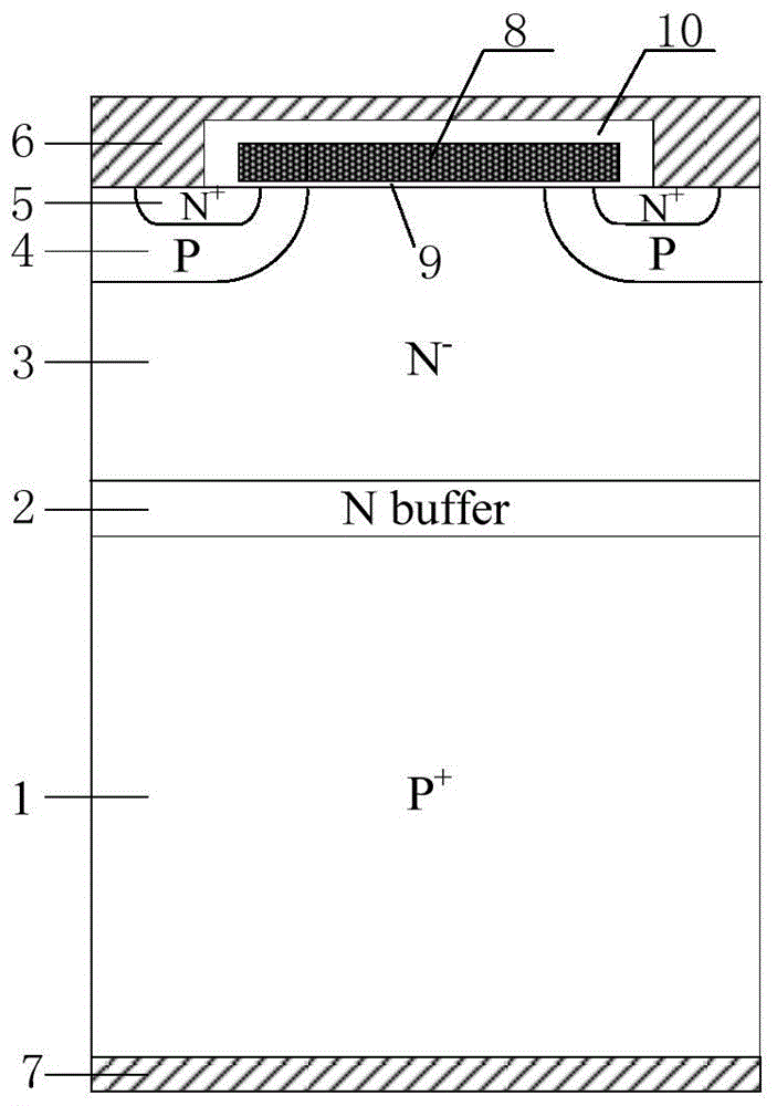
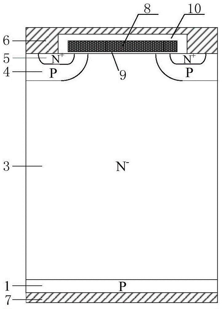
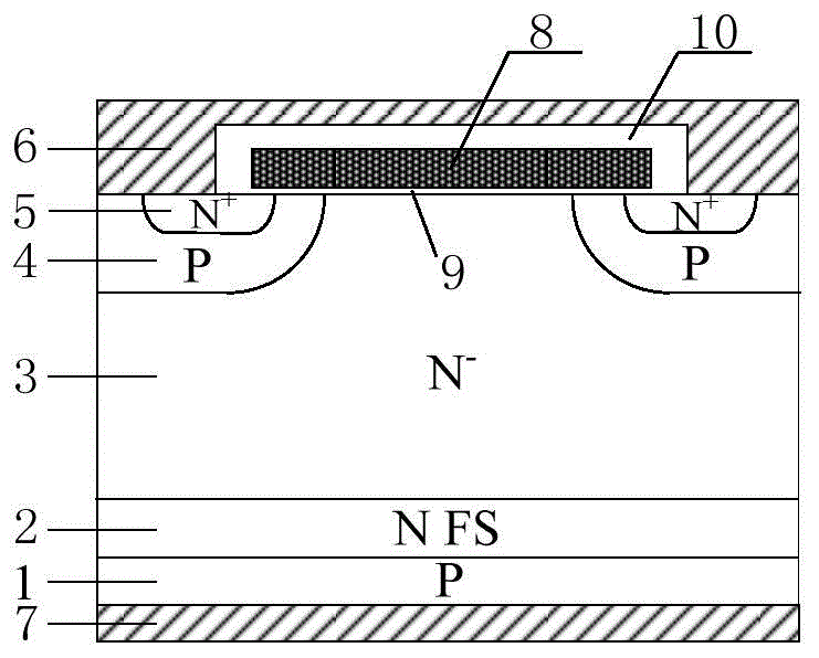
[0039] Such as Figure 6 As shown, the implementation of the present invention provides a method for preparing an FS-IGBT with a thin drift region on a thick silicon wafer, including:

[0040] Step 1: Select two N-type monocrystalline silicon wafers as the first silicon wafer and the second silicon wafer. The thickness of the first silicon wafer is 300 microns, and lightly doped N-type FZ silicon is used with a doping concentration of 2.5* 10 14 piece / cm 3 , to form Figure 5 In the drift region 3 of the FS-IGBT mentioned in the above, the thickness of the second silicon wafer is 300 microns, and heavily doped N-type CZ silicon is used, and the doping concentration is 5*10 19 piece / cm 3 , to ...


PUM

PropertyMeasurementUnit
thicknessaaaaaaaaaa
thicknessaaaaaaaaaa
thicknessaaaaaaaaaa

Abstract

The invention provides a preparation method of an FS-IGBT (Field Stop-Insulated Gate Bipolar Translator), which is used for solving the problems caused by a thin silicon wafer during a preparation process of a medium / low-voltage FS-IGBT that the preparation technology is complicated, the difficulty is large, the thin silicon wafer warps and deforms and is segmented, the size of the thin silicon wafer (a wafer) is limited, the yield is low, the cost is high, and industrialization is difficult to realize and overcoming the huge technical challenge caused by the thin silicon wafer in follow-up scribing of the wafer and encapsulating of a chip. The preparation method comprises the steps of selecting light-doped N-type FZ silicon as a first silicon wafer and heavy-doped N-type or P-type CZ silicon or FZ silicon as a second silicon wafer; firstly, making an N-type FS layer of the FS-IGBT on the back surface of the first silicon wafer, and then, depositing an oxidation layer; bonding the first silicon wafer and the second silicon wafer; making a front-surface structure after thinning the thickness of an original first silicon wafer; etching after thinning the thickness of the second silicon wafer; preparing a P-type transparent collecting zone through a groove; finally, forming a collector electrode through metal depositing and chemical-mechanical polishing; obtaining the FS-IGBT.

Description

technical field [0001] The invention belongs to the technical field of power semiconductor devices, and relates to an insulated gate bipolar transistor (IGBT), in particular to a preparation method of a field stop type insulated gate bipolar transistor (FS-IGBT). Background technique [0002] Insulated gate bipolar transistor (IGBT) is a new type of power electronic device combined with MOS field effect and bipolar transistor. The advantages of large current and low loss have become one of the core electronic components in modern power electronic circuits, and are widely used in various fields of the national economy such as communications, energy, transportation, industry, medicine, household appliances, and aerospace. The invention and application of IGBT have played an extremely important role in improving the performance of power electronic systems. Since the 1990s, through the continuous development of device structure and manufacturing technology, commercial mass-produ...

Claims


Application Information

Patent Timeline
Patent Type & Authority Applications(China)
IPC IPC(8): H01L21/331H01L29/739
Inventor 张金平陈钱刘永郭绪阳朱章丹李泽宏任敏张波
Owner 苏州翠展微电子有限公司
Why Eureka
Try Eureka