High-speed and low-loss multi-trench gate high-voltage power device

A high-voltage power device, low-loss technology, applied in the direction of semiconductor devices, electrical components, circuits, etc., can solve the problems that the devices are not easy to use in parallel, increase the difficulty and cost of the process, increase the distributed resistance, etc., and achieve enhanced injection efficiency and anti-latch lock ability, eliminate the snapback phenomenon, and the effect of fast shutdown speed

Active Publication Date: 2019-11-26
UNIV OF ELECTRONICS SCI & TECH OF CHINA +1
View PDF6 Cites 7 Cited by
  • Summary
  • Abstract
  • Description
  • Claims
  • Application Information

AI Technical Summary

Problems solved by technology

In order to reduce the turn-off loss of LIGBT devices E off , Shorted Anode (Shorted Anode, SA) LIGBT introduces the N+ collector area at the collector end, which provides a fast extraction channel for electrons during the turn-off process to accelerate the turn-off of the device and reduce E off , but this also leads to the snapback effect in the on-state of the device, which makes it difficult for the device to be used in parallel and reduces reliability
In order to eliminate the snapback effect, the literature Long Zhang, JingZhu, Weifeng Sun, et al.A High Current Density SOI-LIGBT with SegmentedTrenches in the Anode Region for Suppressing Negative Differential ResistanceRegime, IEEE ISPSD, 2015 P+ collector area and N+ collector area Segmented dielectric isolation slots are introduced between them, and the electronic current path is compressed by reducing the spacing of the dielectric isolation slots, thereby increasing the distributed resistance to eliminate the snapback effect; the slot spacing must be small enough to eliminate snapback, but the corresponding N+ collector region is turned off during The efficiency of extracting electrons will also decrease, and the fabrication of deep grooves will increase the difficulty and cost of the process

Method used


Image

  • High-speed and low-loss multi-trench gate high-voltage power device
  • High-speed and low-loss multi-trench gate high-voltage power device
  • High-speed and low-loss multi-trench gate high-voltage power device

Examples


Embodiment 1

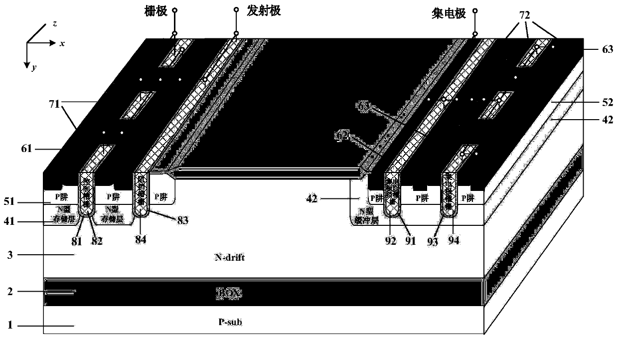
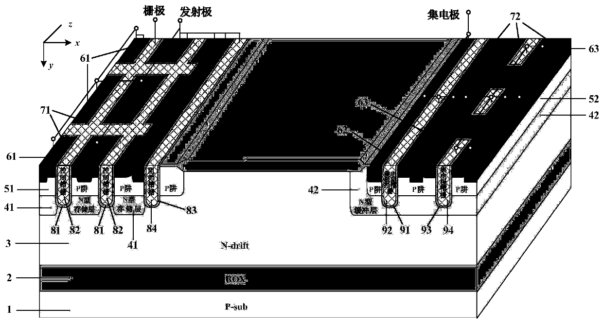
[0016] Such as figure 1 As shown, the multi-groove gate SOI LIGBT of this example includes a bottom-up substrate layer 1, an insulating dielectric layer 2, and an N-type drift region 3; one end of the N-type drift region 3 includes an emitter structure and an emitter groove structure, and the other end includes a collector structure and a collector tank structure.

[0017] The emitter structure includes a P well region 51, a P+ body contact region 61, and an N+ emitter region 71; the P+ body contact region 61 and the N+ emitter region 71 are located on the top of the P well region 51, and the P+ body The common lead end of the contact region 61 and the N+ emitter region 71 is the emitter; the collector structure includes the N-type buffer layer 42, the P well region 52, the P+ collector region 62, the N+ collector region 72 and the P well region 52 The body contacts the P+ region 63, the N-type buffer layer 42 is located on the top of the N-type drift region 3, the P well reg...

Embodiment 2

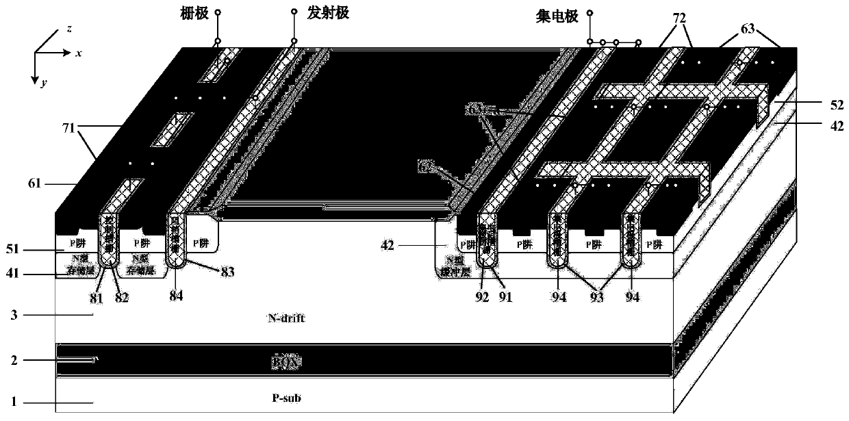
[0024] Such as Image 6 Shown, in this example and embodiment 1 figure 1 The difference is that in this example, a P-type buried layer 53 is introduced under the trench gate structure at the emitter terminal. The working mechanism of device shutdown in this embodiment is consistent with that of Embodiment 1, the difference is that: when conducting forward conduction, the P-type buried layer 53 introduced in this example can assist in depleting the N-type storage layer 41, thereby improving the efficiency of the N-type storage layer. 41 Optimize the doping concentration and enhance the carrier storage effect, so in this example, the carrier concentration in the drift region of the device is higher, and the conduction voltage drop can be further reduced; at the same time, in the blocking state, the P-type buried layer 53 can also The electric field peak at the bottom of the emitter terminal groove structure is reduced, and the reliability of the device is improved. Therefore, ...


PUM


Abstract

The invention belongs to the technical field of power semiconductors and particularly relates to a high-speed and low-loss multi-trench gate high-voltage power device. Compared with a traditional structure, the structure of the high-speed and low-loss multi-trench gate high-voltage power device has the advantage that a plurality of trench gate structures are introduced into an emitter terminal anda collector terminal. Channels in side walls of trench gates at the collector terminal are turned off and a connection path of an N+ collector region and an N-type buffer layer is blocked during forward conduction, so that the voltage foldback effect can be eliminated. A trench gate structure at the emitter terminal can increase the channel density to reduce the resistance of a channel region, and a barrier trench gate and a carrier storage layer can effectively improve the carrier concentration of a drift region, so that the novel device can obtain lower forward conduction voltage drop. In the turn-off process, the channels in the side walls of the trench gates at the collector terminal are opened along with voltage rise of a collector, so that the N+ collector region communicates with the N-type buffer layer to form a rapid electron extraction path and turn-off of the device is accelerated to reduce the turn-off loss. Therefore, the high-speed and low-loss multi-trench gate high-voltage power device has lower forward conduction voltage drop and smaller turn-off loss and does not have the voltage foldback effect.

Description

technical field [0001] The invention belongs to the technical field of power semiconductors, and relates to a multi-groove gate SOI LIGBT (Lateral Insulated Gate Bipolar Transistor, lateral insulated gate bipolar transistor). Background technique [0002] Insulated gate bipolar transistor (IGBT) is a voltage-controlled bipolar conductive device, which has the advantages of high input impedance of MOS gate-controlled devices, simple driving circuit, low driving power consumption, high current density of bipolar devices, and reduced conduction voltage. It is one of the core electronic components in the medium and high power field, and is widely used in rail transit, smart grid, aerospace, electric vehicles, household appliances and new energy equipment and other fields. Because SOI technology has the advantages of small leakage current, easy isolation, and small parasitic effects, SOIL IGBT is the core component of a monolithic power integrated chip. [0003] The LIGBT device...

Claims


Application Information

Patent Timeline
Patent Type & Authority Applications(China)
IPC IPC(8): H01L29/739H01L29/08
CPCH01L29/0804H01L29/7394H01L29/7397
Inventor 魏杰黄俊岳马臻王晨霞鲁娟郗路凡宋旭罗小蓉杨永辉朱坤峰
Owner UNIV OF ELECTRONICS SCI & TECH OF CHINA
Why Eureka
Try Eureka