Inspection method and apparatus for mounted electronic components

A technology of electronic components and inspection methods, applied in the direction of electrical components, measuring devices, optical devices, etc., can solve the problems of not being able to take pictures, spending a lot of effort and time, and not being able to respond appropriately immediately, and achieve efficient installation and inspection Effect

Active Publication Date: 2006-08-16
FUJI MASCH MFG CO LTD
View PDF2 Cites 16 Cited by
  • Summary
  • Abstract
  • Description
  • Claims
  • Application Information

AI Technical Summary

Problems solved by technology

Therefore, it is not possible to photograph all of the multiple components mounted on the substrate at one time. In addition, when the mounted components are large components, the entire range of the large components cannot be photographed. Therefore, in order to detect all the components mounted on the substrate In case of abnormal installation of parts and abnormal installation of large parts, it is necessary to combine many captured images, which requires a lot of work and time for image processing
[0007] In addition, in the inspection device of the above-mentioned Patent Document 2, since the device for mounting the electronic component on the substrate and the device for inspecting the mounting state of the electronic component mounted on the substrate are provided separately, there is a possibility that even if an abnormality is found in the mounting state Disadvantages of not being able to respond appropriately immediately

Method used


Image

  • Inspection method and apparatus for mounted electronic components
  • Inspection method and apparatus for mounted electronic components
  • Inspection method and apparatus for mounted electronic components

Examples


Embodiment Construction

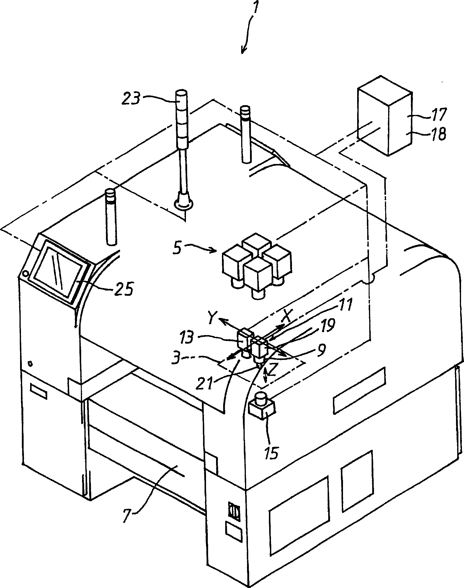
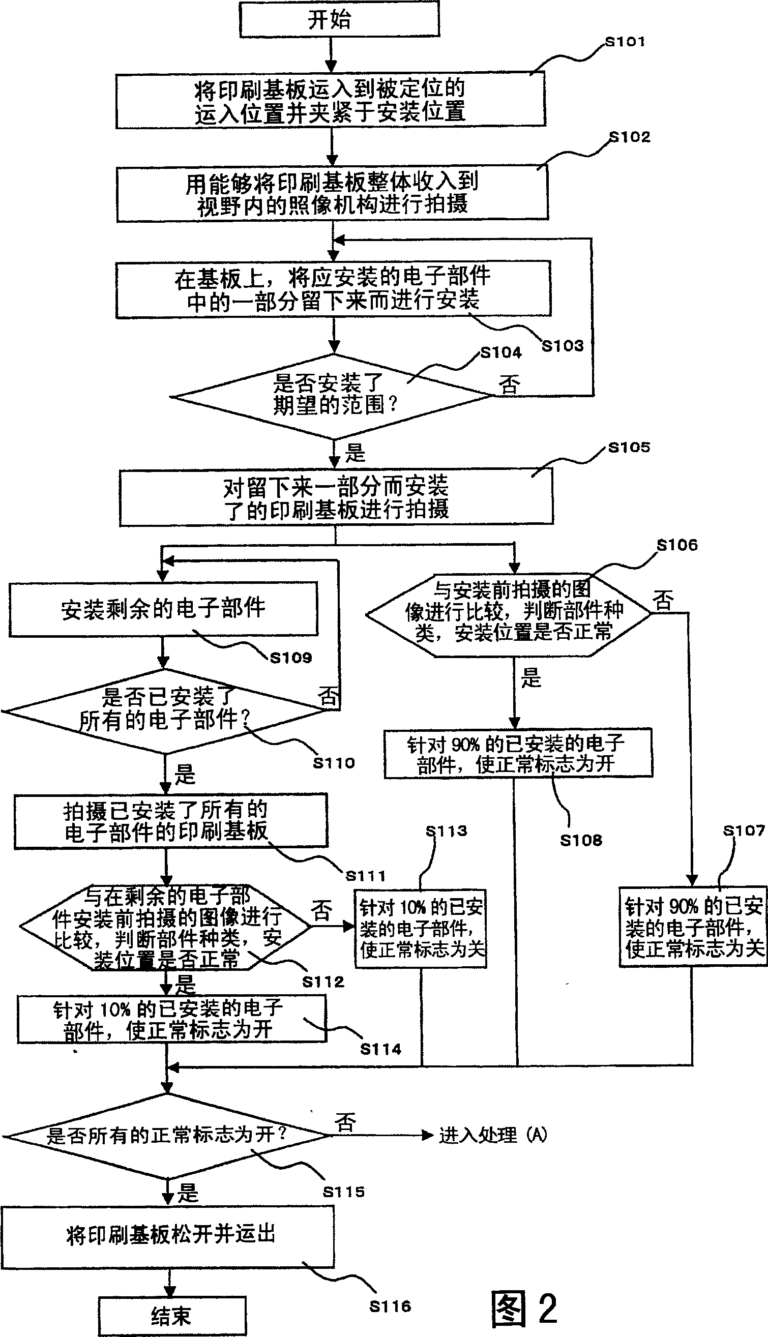
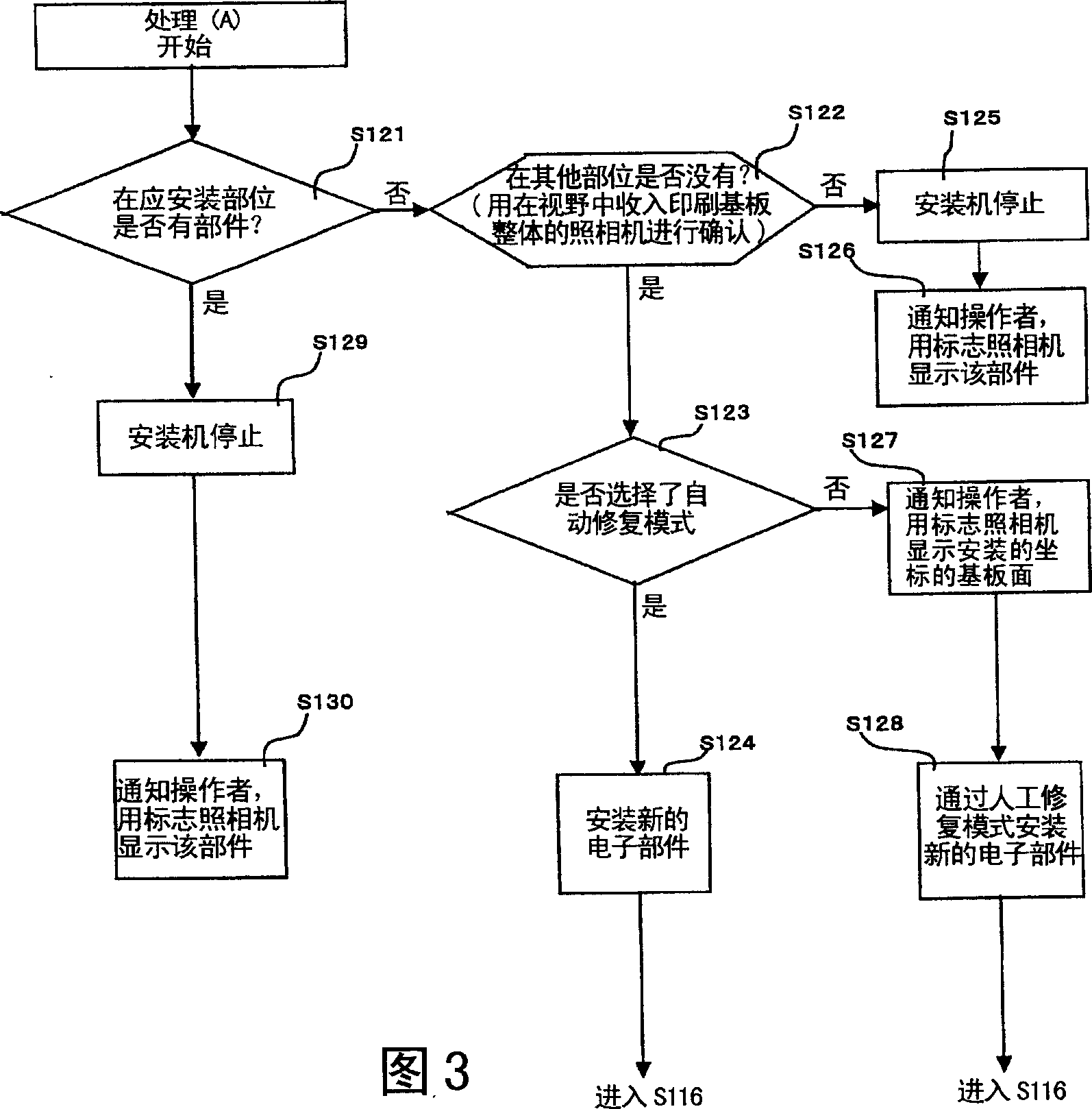
[0040] Hereinafter, a first embodiment of the inspection method and device of a mounted electronic component according to the present invention will be described based on the drawings. figure 1 It is a schematic perspective view showing a mounting machine 1 equipped with an inspection device for inspecting mounted electronic components 2 .

[0041] The mounting machine 1 to which this inspection device is installed includes: a camera device 5 consisting of a camera capable of taking in the entirety of the printed circuit board 3 carried in and positioned and placed in a predetermined position into the field of view at one time; Not shown in the drawing, it carries the printed circuit board 3 into the carrying position and positions it at a predetermined position; it is provided on a movable table (not shown) supported so as to be movable in the X and Y directions with respect to the base 7 The component transfer device 11 of the component mounting head 9 and the substrate reco...


PUM


Abstract

The invention provides a method and a system for inspecting mounted electronic components, capable of simultaneously imaging electronic components to be mounted to a printed circuit board, and speedily and appropriately processing mounting defects. The system for inspecting mounted electronic components is provided with a camera means, capable of keeping an overall printed circuit board within its field of view. The overall printed circuit board is imaged by the camera means at first time prior to mounting. heaving a part of the electronic components to be mounted to the board, the electronic components are mounted. The overall printed circuit board, mounted with the electronic components to be mounted except the part of them, is imaged with the camera means the second time. In image processing for determining component mounting quality, images imaged at the second time are compared with the images imaged at the first time to determine the correctness of the component type and mounting positions of the electronic components mounted to the printed circuit board prior to the second imaging. The remaining electronic components are mounted to the printed circuit board, in parallel with the image processing.

Description

technical field [0001] The present invention relates to an inspection method and device for inspecting whether the type of electronic components mounted on a printed circuit board is good or not, and whether the mounting position is good or not. Background technique [0002] Conventionally, the technology of Patent Document 1 has been known as a method for inspecting the quality of mounting of electronic components mounted on a printed circuit board. In this technology, the printed circuit board P2 on which the electronic components W have been mounted is transported along the table 2 by the mounting spindle 3 at the mounting position of the table 2 and positioned to the inspection position on the downstream side. The substrate P1 is carried in again and positioned at the mounting position of the table 2, and in this state, mounting to the printed circuit board P1 at the mounting position and inspection of the mounting state of the printed circuit board P2 at the inspection ...

Claims


Application Information

Patent Timeline
Patent Type & Authority Applications(China)
IPC IPC(8): G01B11/00G06T7/00
CPCY10T29/53087H01L21/67259G06T7/001Y10T29/4913Y10T29/53178Y10T29/49133G06T2207/30141H01L21/67144Y10T29/49131
Inventor 河田东辅
Owner FUJI MASCH MFG CO LTD
Why Eureka
Try Eureka