CMOS image sensor and method for fabricating the same

An image sensor and device technology, applied in semiconductor/solid-state device manufacturing, electrical solid-state devices, semiconductor devices, etc., can solve problems such as limitation and difficulty in preventing dark current

Inactive Publication Date: 2006-08-16
DONGBUANAM SEMICON
View PDF0 Cites 15 Cited by
  • Summary
  • Abstract
  • Description
  • Claims
  • Application Information

AI Technical Summary

Problems solved by technology

Therefore, in the CMOS image sensor of the related art, it is difficult to prevent the dark current generated in the boundary portion between the device isolation film and the active region of the photodiode region
This limits the improvement of the characteristics related to dark current

Method used


Image

  • CMOS image sensor and method for fabricating the same
  • CMOS image sensor and method for fabricating the same
  • CMOS image sensor and method for fabricating the same

Examples


Embodiment Construction

[0045] Reference will now be made in detail to the preferred embodiments of the invention, examples of which are illustrated in the accompanying drawings. Wherever possible, the same reference numbers will be used throughout the drawings to refer to the same or like parts.

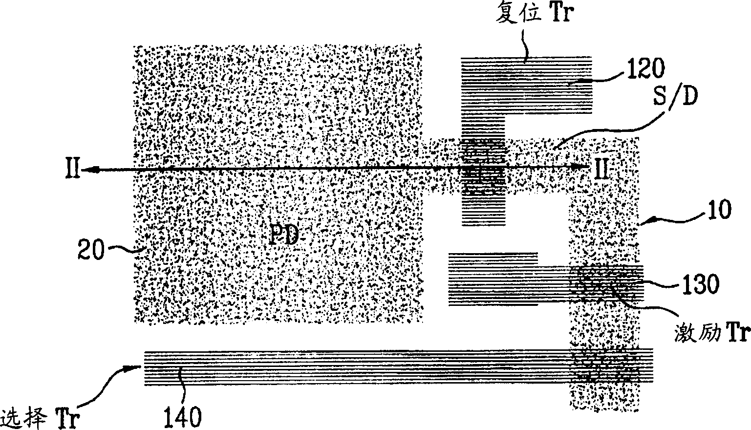
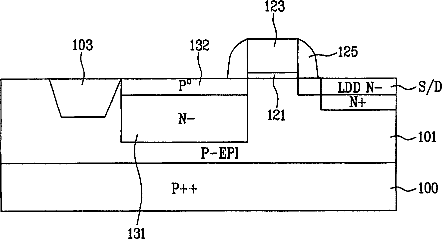
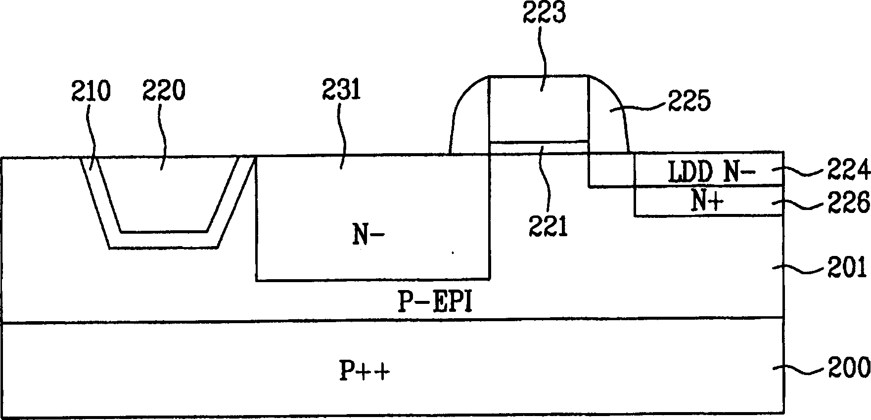
[0046] image 3 is a cross-sectional view similar to FIG. 2, showing a photodiode and a transfer transistor of a CMOS image sensor according to the present invention.

[0047] Such as image 3 As shown, in the p defined by the active region 10 (see Figure 1) and the device isolation region ++ type semiconductor substrate 200 to form P - type epitaxial layer 201 . A device isolation film 220 , that is, a shallow trench isolation (STI) film is formed in a device isolation region over the semiconductor substrate 200 .

[0048] The active region of the semiconductor substrate 200 is defined by the photodiode region PD and the transistor region.

[0049] The gate electrode 223 of the transfer transistor 120...


PUM


Abstract

A CMOS image sensor and a method for fabricating the same are disclosed, in which a dark current is prevented from being generated between a device isolation film and a photodiode region to improve characteristics of the image sensor.

Description

[0001] This application claims priority from Korean Patent Application No. P2004-114660 filed on December 29, 2004, the entire contents of which are hereby incorporated by reference. technical field [0002] The present invention relates to a complementary metal oxide semiconductor (CMOS) image sensor and a manufacturing method thereof, and more particularly, to a CMOS image sensor and a manufacturing method thereof that prevent dark current from occurring, thereby improving characteristics of the image sensor. Background technique [0003] Generally, an image sensor is a semiconductor device that converts an optical image into an electrical signal. Image sensors include charge-coupled devices (CCDs) and CMOS image sensors. [0004] The CCD includes: a plurality of photodiodes PD arranged in a matrix for converting optical signals into electrical signals; a plurality of vertical charge-coupled devices (VCCDs) formed between the photodiodes in the vertical direction for trans...

Claims


Application Information

Patent Timeline
Patent Type & Authority Applications(China)
IPC IPC(8): H01L27/146H01L21/822
CPCH01L27/1463H01L27/14643H01L27/14609H01L27/14689H01L27/146H01L31/10
Inventor 韩昌勋
Owner DONGBUANAM SEMICON
Why Eureka
Try Eureka