Semiconductor device and manufacturing method thereof

A manufacturing method and semiconductor technology, which are applied in the fields of semiconductor/solid-state device manufacturing, semiconductor devices, electric solid-state devices, etc., to achieve the effect of not being damaged easily

Active Publication Date: 2010-09-29
AOI ELECTRONICS CO LTD
View PDF3 Cites 0 Cited by
  • Summary
  • Abstract
  • Description
  • Claims
  • Application Information

AI Technical Summary

Problems solved by technology

[0003] However, in the semiconductor device obtained by the above-mentioned conventional manufacturing method, there is the following problem: if the back surface of the semiconductor substrate is ground, a Even if a protective film made of resin is formed on the fine and acute-angled concave-convex surface, it is difficult to reliably fill the depth of the fine and acute-angled concave portion, because the depth of the fine and acute-angled concave portion is not covered. Due to the protective film covering, there is a possibility of damage to the back surface of the semiconductor substrate

Method used


Image

  • Semiconductor device and manufacturing method thereof
  • Semiconductor device and manufacturing method thereof
  • Semiconductor device and manufacturing method thereof

Examples


no. 1 Embodiment approach

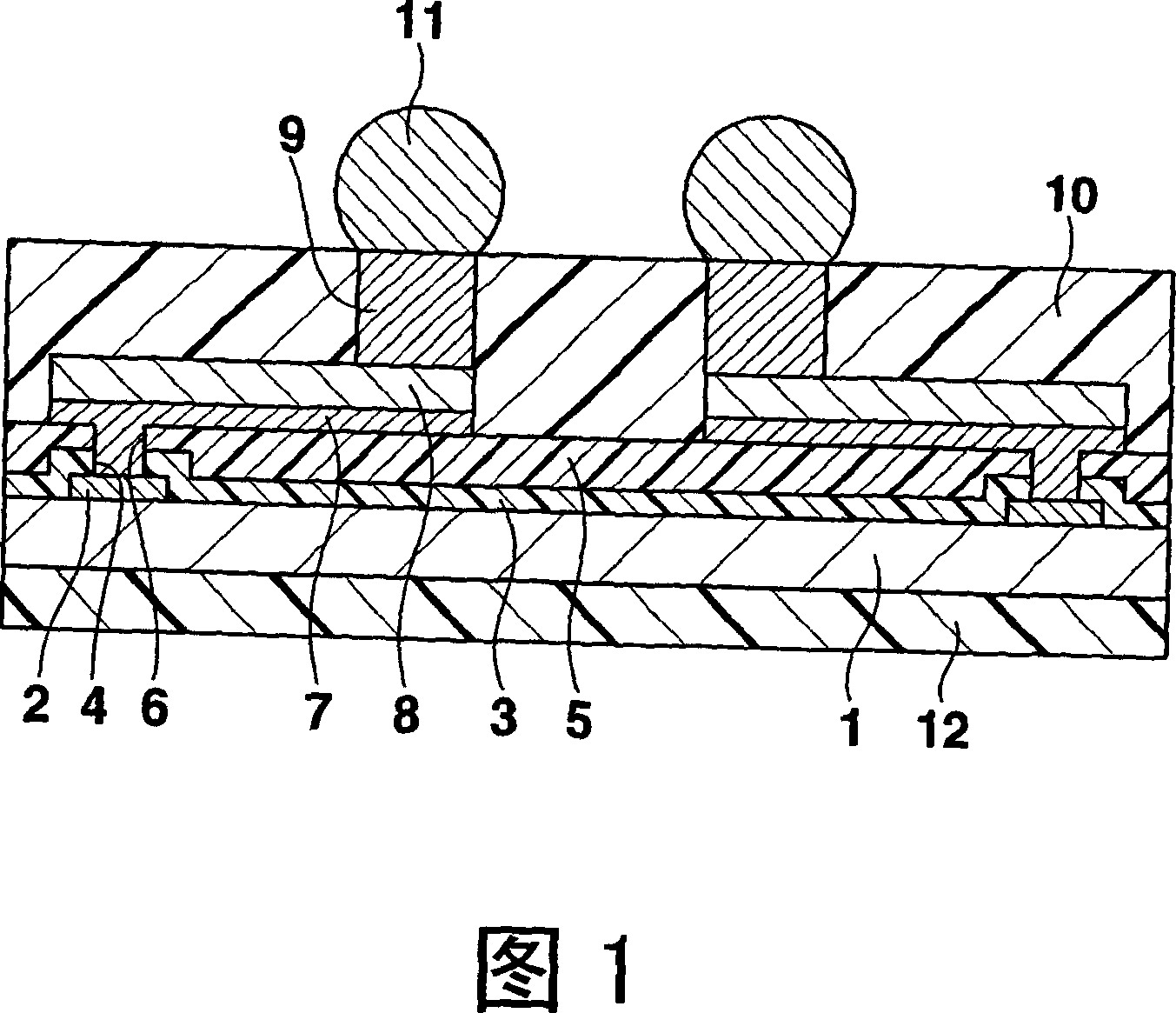
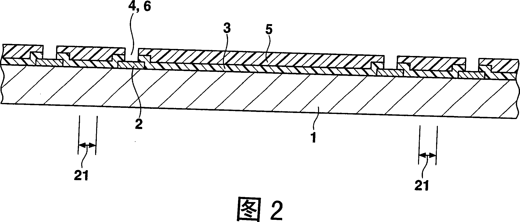
[0037] figure 1 A cross-sectional view of a semiconductor device as an embodiment of the invention is shown. This semiconductor device is generally called a CSP (chip size package), and includes a silicon substrate (semiconductor substrate) 1 . An integrated circuit (not shown) having a predetermined function is provided on the upper surface of the silicon substrate 1 , and a plurality of connection pads 2 made of aluminum-based metal or the like are provided on the periphery of the upper surface to connect to the integrated circuit.

[0038] An insulating film 3 made of silicon oxide or the like is provided on the upper surface of the silicon substrate 1 except for the central portion of the connecting pad 2, and the central portion of the connecting pad 2 is opened through the opening 4 provided in the insulating film 3. exposed. A protective film 5 made of epoxy resin, polyimide resin, or the like is provided on the upper surface of the insulating film 3 . In this case,...

no. 2 Embodiment approach

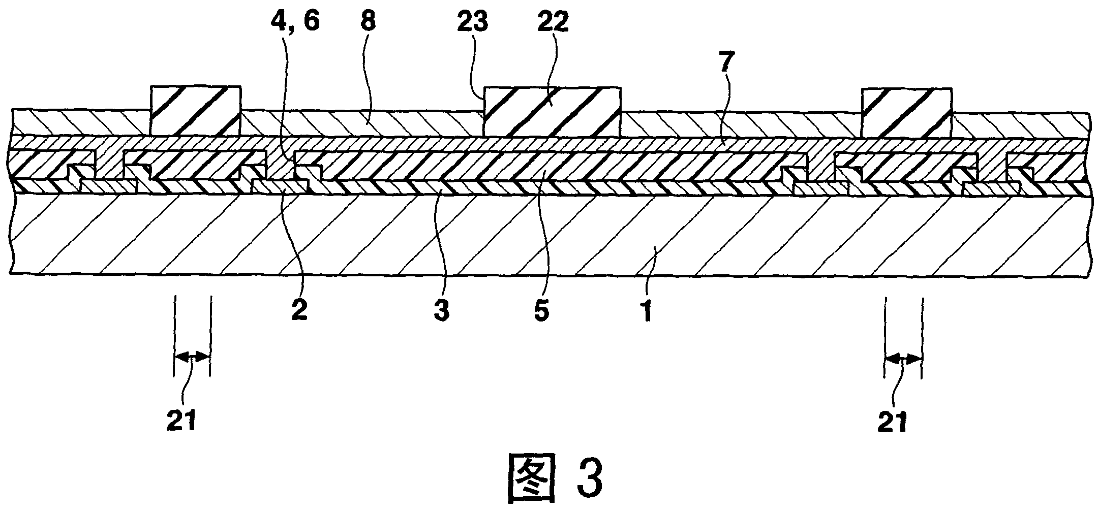
[0056] Figure 14 The second embodiment of the invention is shown. An integrated circuit (not shown) with a predetermined function is provided on the upper surface of the silicon substrate, and a plurality of connection pads 2 made of aluminum-based metal or the like are provided on the periphery of the upper surface to connect to the integrated circuit.

[0057] An insulating film 3 made of silicon oxide or the like is provided on the upper surface of the substrate 1 , and the central portion of the connection pad 2 is exposed through an opening 4 provided in the insulating film 3 . A protective film 5 made of epoxy resin or polyimide resin is provided on the upper surface of the insulating film 3 . In this case, an opening 6 is provided in a portion of the protective film 5 corresponding to the opening 4 of the insulating film 3 .

[0058] A base metal layer 7 made of copper or the like is provided on the upper surface of the protective film 5 . Wiring 8 made of copper is...


PUM


Abstract

A fabrication process for semiconductor device, aimed to retard cracking in the lower surface of a silicon substrate subjected to grinding. A silicon substrate 1 is ground appropriately on the lower surface side. Consequently, fine and acute protrusions and recesses (crystal destruction layer of silicon) are formed on the lower surface of the silicon substrate 1. The lower surface of the silicon substrate 1 is then roughened with level difference of 1-5 [mu]m by wet etching. Subsequently, a protective film 12 is formed of epoxy based resin, or the like, on the lower surface of the silicon substrate 1. Since the lower surface of the silicon substrate 1 is roughened with level difference of 1-5 [mu]m, the rough surface is covered surely with the protective film 12 and cracking is retarded in the lower surface of the silicon substrate.

Description

technical field [0001] The present invention relates to a semiconductor device and a method of manufacturing the same. Background technique [0002] Along with the thinning of electronic equipment, the thinning of semiconductor devices is required. However, if the semiconductor substrate in the wafer state is thinned excessively, the semiconductor substrate may be damaged during a so-called semiconductor manufacturing process in which an integrated circuit is formed on the front surface of the semiconductor substrate in the wafer state. Therefore, a method of reducing the thickness of the semiconductor substrate by grinding the back surface opposite to the surface on which the integrated circuits are formed after forming integrated circuits on the front surface of a semiconductor substrate in a wafer state has been developed. Japanese Patent Laid-Open No. 2001-230224 discloses such a conventional semiconductor device manufacturing method. This previous document discloses ...

Claims


Application Information

Patent Timeline
Patent Type & Authority Patents(China)
IPC IPC(8): H01L27/04H01L21/822
CPCH01L2924/14H01L2224/023H01L2224/11H01L2924/0001
Inventor 若林猛三原一郎
Owner AOI ELECTRONICS CO LTD
Why Eureka
Try Eureka