CMOS image sensor for reducing partition noise
An image sensor, pixel technology, applied in image communication, electric solid state devices, semiconductor devices, etc., can solve the problem of short turn-off time of transfer transistor TX
- Summary
- Abstract
- Description
- Claims
- Application Information
AI Technical Summary
Problems solved by technology
Method used
Image

Examples
Embodiment 1
[0050] The first embodiment increases the falling time of the transfer control signal applied to the gate of the transfer transistor by reducing the W / L ratio of the NMOS transistor of the CMOS type driver DRV.
[0051] 7A to 7C are circuit diagrams describing a driver for controlling a transfer transistor according to a first embodiment of the present invention.
[0052] The CMOS inverter type driver shown in FIG. 7A includes a PMOS transistor P and an NMOS transistor N connected in series between a power supply voltage VDD and a ground voltage VSS. The CMOS inverter type driver receives an input signal IN through the gates of these two transistors to show an inverted signal OUT.
[0053] Assuming that the W / L ratio of the NMOS transistor N is K, by increasing the length L or decreasing the width W, the resistance can be increased, that is, the current can be reduced, thereby increasing the fall time of the transfer control signal.
[0054] Meanwhile, the width W of the gate...
Embodiment 2
[0063] The second embodiment increases the fall time (τ) of the transfer transistor by adding a capacitor C. FIG.
[0064] Figure 9 and 10 is a diagram describing a CMOS type driver for driving a transfer transistor according to a second embodiment of the present invention.
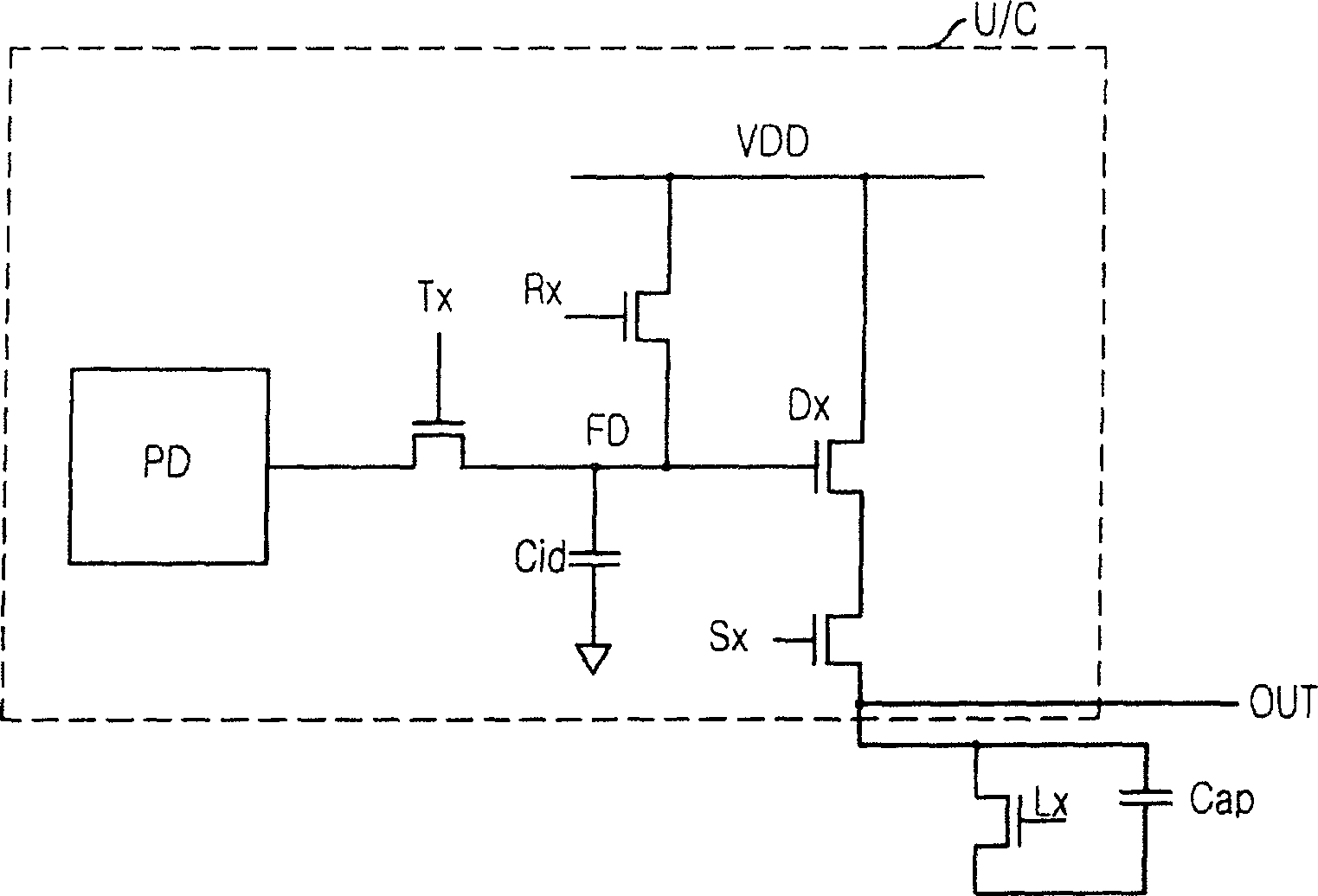
[0065] As shown, the CMOS image sensor includes a plurality of unit pixels P1 to P1280 and a CMOS type driver DRV. Each unit pixel P1 to P1280 includes a photodiode, a floating diffusion node, a transfer transistor, a reset transistor, a driving transistor, and a selection transistor. The CMOS type driver DRV controls the turn-on and turn-off operations of the transfer transistors TX1 to TX1280 included in the unit pixel.
[0066] As an example of the CMOS type driver DRV, a CMOS inverter type driver is shown. A plurality of unit pixels P1 to P1280 are arranged in a single row. Accordingly, the CMOS type driver DRV simultaneously controls a plurality of transfer transistors TX1 to TX1280 of unit pix...
Embodiment 3
[0074] By partially modifying the structure of the first embodiment, the layout can be designed more simply.
[0075] Figures 11A to 11C is a circuit diagram of a driver for controlling a transfer transistor according to a third embodiment of the present invention.
[0076] As shown, the CMOS inverter type driver includes one PMOS transistor P111 and four NMOS transistors N111 to N114 connected in series.
[0077] Although the basic structure is similar to that of FIG. 7C, the sources of the NMOS transistors N111 to N114 are commonly connected to the ground voltage VSS, thereby forming a kind of resistor.
[0078] exist Figure 11A , the sources of the NMOS transistors N111 to N114 are commonly connected to the ground voltage VSS. exist Figure 11B , the sources of the NMOS transistors N112 to N114 are commonly connected to the ground voltage VSS. exist Figure 11C In , the source of no NMOS transistor is connected to the ground voltage VSS.
[0079] exist Figures 11...
PUM
 Abstract
Description
Claims
Application Information
 - R&D
- Intellectual Property
- Life Sciences
- Materials
- Tech Scout
- Unparalleled Data Quality
- Higher Quality Content
- 60% Fewer Hallucinations
Browse by: Latest US Patents, China's latest patents, Technical Efficacy Thesaurus, Application Domain, Technology Topic, Popular Technical Reports.
© 2025 PatSnap. All rights reserved.Legal|Privacy policy|Modern Slavery Act Transparency Statement|Sitemap|About US| Contact US: help@patsnap.com