
Monitor element and magneto-resistance effect element substrate, and method of manufacturing monitor element

A technology of magnetoresistance effect element and manufacturing method, which is applied in the direction of manufacturing magnetic head surface, magnetic flux-sensitive magnetic head, magnetic recording head, etc., can solve the problems of shape deformation, difficult separation process and peeling of the opposite surface of the medium, and achieve the purpose of preventing short circuit Effect

Inactive Publication Date: 2006-09-13
TDK CORPARATION
View PDF2 Cites 2 Cited by
  • Summary
  • Abstract
  • Description
  • Claims
  • Application Information

AI Technical Summary

Problems solved by technology

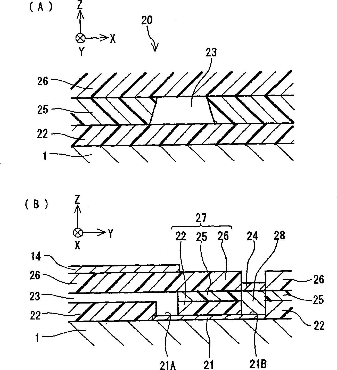
[0006] However, in the monitoring element of the above-mentioned prior art, due to the excessive amount of etching processing when removing the electroplating bottom film, the etching process exposes the electrode layer between the upper shielding layer and the electrode terminal, and it is easy to be exposed between the electrode layer and the upper shielding layer. A short circuit (short) occurs between the shielding layers
In order to prevent this phenomenon, although it is possible to increase the film thickness of the second additional void layer formed on the electrode layer, if the second additional void layer is thickened, the second additional void layer will be formed by separation. Difficulty in the lift-off process, resulting in deformation of the shape exposed on the surface facing the medium, or causing problems such as peeling off

Method used


Image

  • Monitor element and magneto-resistance effect element substrate, and method of manufacturing monitor element
  • Monitor element and magneto-resistance effect element substrate, and method of manufacturing monitor element
  • Monitor element and magneto-resistance effect element substrate, and method of manufacturing monitor element

Examples


Embodiment Construction

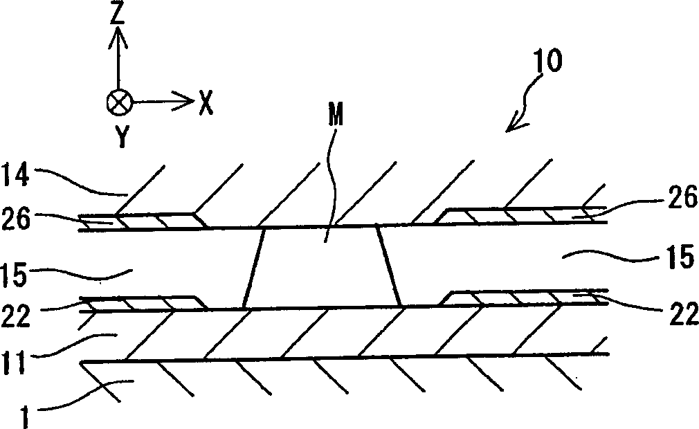
[0032] The present invention is illustrated below with reference to the accompanying drawings. In each figure, the X direction is the width direction of the track (track), the Y direction is the element height direction (the leakage field direction from the recording medium), and the Z direction is the moving direction of the recording medium and each layer constituting the magnetoresistance effect element. Stacking direction.

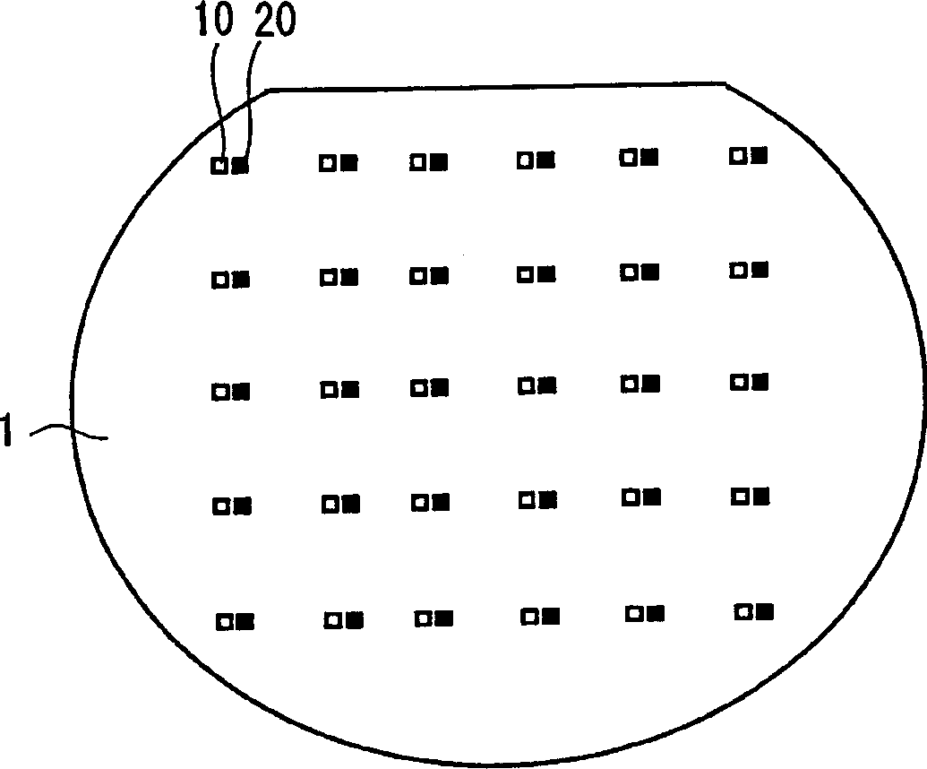
[0033] figure 1 It is a schematic diagram showing a wafer according to one embodiment of the present invention. A plurality of CPP-type magnetoresistance effect elements 10 are formed in parallel on a wafer 1, and monitoring elements 20 that are located near each CPP-type magnetoresistance effect element 10 and paired with the CPP-type magnetoresistance effect elements 10 are respectively formed. . exist figure 1 In , the CPP type magnetoresistive effect element 10 is indicated by □, and the monitor element 20 is indicated by ■.

[0034] CPP type ...


PUM


Abstract

The objective of the invention is to provide a monitor element and a magneto-resistance effect element substrate which can be prevented from short circuits, and also to provide a method of manufacturing the monitor element. The monitor element is used as an element resistance monitor for a magneto-resistance effect element during a polishing process for forming the medium facing surface of the magneto-resistance effect element which is applied with sensing current in a direction perpendicular to a film surface by upper and lower shield layers. The monitor element comprises a multilayer film having the same film structure as a magneto-resistance effect film of the magneto-resistance effect element, and an electrode layer which applies current in parallel to the film surface of the multilayer film. The electrode layer is formed at the same height as the lower shield layer, and is covered with an insulating protection layer except for an electrode connecting portion with the multilayer film and an electrode extractor.

Description

technical field [0001] The present invention relates to a monitor (monitor) element used for grinding a medium-facing surface (media-facing surface) of a CPP type magnetoresistance effect element and a magnetoresistance effect element substrate (magnetoresistive effect element) provided with the monitor element. substrate), and a method of manufacturing a monitoring element. Background technique [0002] A magnetoresistive element is an element that reads a change in the intensity of an external magnetic field as a change in voltage when a constant current flows, and is widely used in hard disk devices, magnetic sensors, and the like. Conventionally, in order to improve productivity, the element structure of a plurality of magnetoresistive effect elements is formed side by side on one wafer (substrate), and then the wafer is cut, and the medium-facing surface is formed by grinding (limiting the height of the element), thereby Obtain a wafer bar (wafer bar) (strip-shaped mag...

Claims


Application Information

Patent Timeline
Patent Type & Authority Applications(China)
IPC IPC(8): G11B5/39G11B5/187
Inventor 高桥亨
Owner TDK CORPARATION
Learn More