
Anti-welding procedue of PCB

A technology of anti-soldering and baking paint, which is applied in the fields of printed circuit manufacturing, printed circuit secondary treatment, electrical components, etc., and can solve problems such as low stability, multi-process equipment, increased investment and production costs, etc.

Inactive Publication Date: 2006-09-20
杨合卿
View PDF0 Cites 6 Cited by
  • Summary
  • Abstract
  • Description
  • Claims
  • Application Information

AI Technical Summary

Problems solved by technology

[0004] 1. More consumables are used, and the manufacturing time is longer, which increases the cost
[0005] 2. The thick and thin ink coating is uneven, which is prone to impedance changes and affects electrical characteristics
[0006] 3. Because the ink is required to be coated evenly, it is necessary to use more sophisticated equipment, which increases investment and production costs
[0007] 4. Since the existing process is image transfer technology, more equipment is used and the process is longer
[0008] 5. Since the film used is quite sensitive to the ambient temperature, there will be a difference in size with the change of the ambient humidity, and the stability is low
[0009] In addition, the existing solder mask structure is monotonous in color, lacks change and is easy to scratch, which is not ideal

Method used


Image

  • Anti-welding procedue of PCB
  • Anti-welding procedue of PCB
  • Anti-welding procedue of PCB

Examples


Embodiment Construction

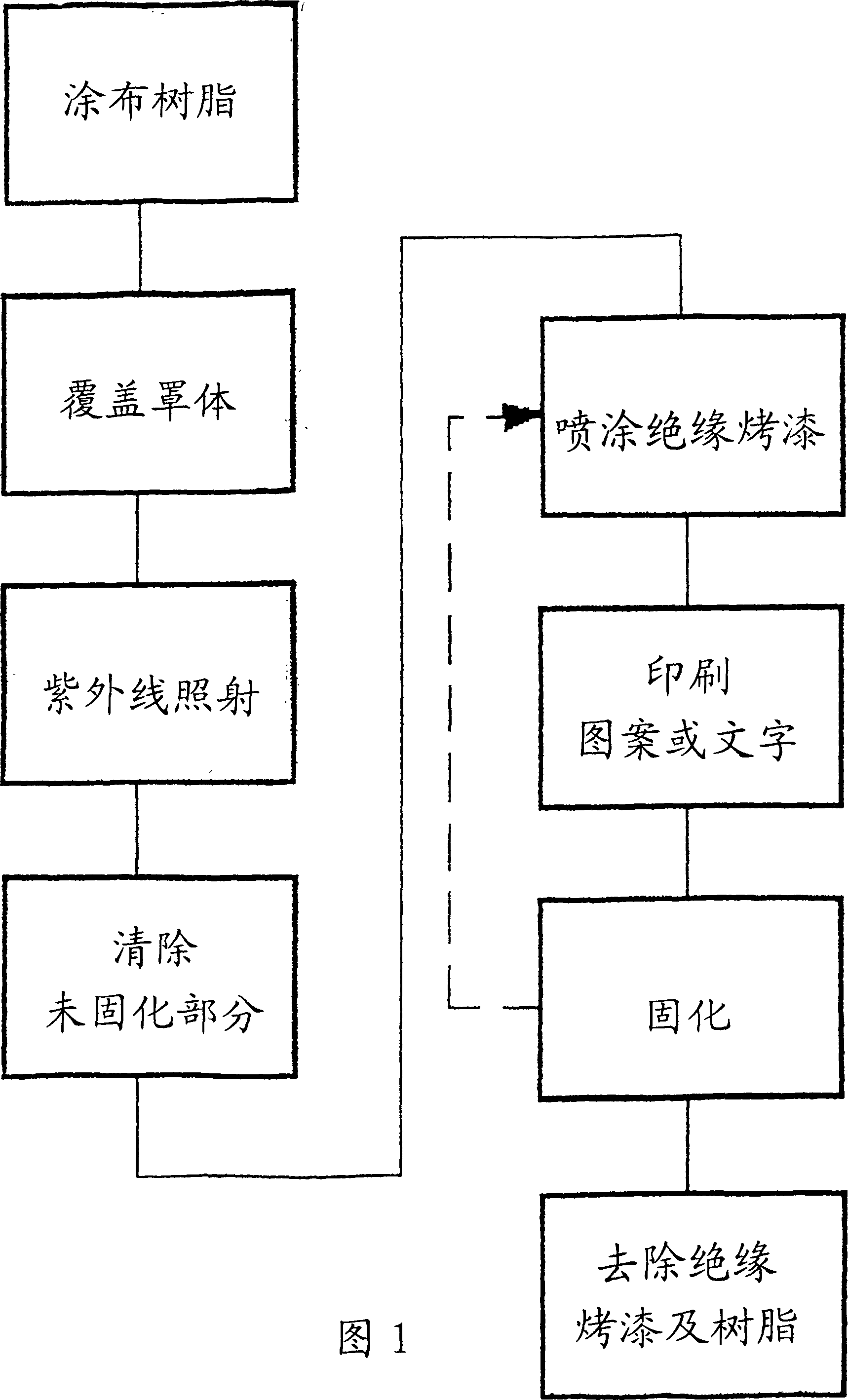
[0025] As shown in Figure 1, the present invention mainly comprises the following steps:

[0026] A. Coating resin:

[0027] Such as figure 2 , image 3 As shown, make a steel plate according to the required pattern, open a larger hole on the position to be exposed on the steel plate, and apply the low-hardness resin 1 to the part of the PCB 2 where the contact 21 is to be exposed through the steel plate, so that the coating area needs to be larger than the contact 21 area and need to completely cover the contact point 21.

[0028] B. Covering the cover body:

[0029] Make the covering steel plate according to the requirements, open the position of the part to be exposed according to the size required by the graphic, and cover the covering steel plate on the resin-coated PCB 2.

[0030] C. Ultraviolet radiation and removal of uncured parts:

[0031] After being irradiated with ultraviolet rays, the resin in the opening part is cured, and the resin can also be cured by bak...


PUM


Abstract

The invention provides an improved solder mask structure to prevent the variation of electrical character and comprises: the step of coating the resin, making a steel plate with a large hole on the portion to be exposed, the resin is coated on the contact portion to be exposed and totally covers the contact portion; the step of covering mask, making a steel plate for coverage on which a hole in a designed size is opened, and covering the steel plate for coverage on the coated resign; the step of ultraviolet radiation, after ultraviolet radiation, the resin on the portion of opening hole is solidified; the step of spraying insulation finish, spraying the insulation finish on the PCB, and then solidifying it; the step of removing the insulation finish and resin, removing the insulation finish and resin on contact portion to be exposed using dull polish or sand blast; after washing, the contact portion is kept an exposing state, and other portion of the PCB is covered by the insulation finish.

Description

technical field [0001] The invention belongs to an auxiliary manufacturing method for circuit board manufacturing, in particular to a PCB solder-proof process. Background technique [0002] In the existing PCB solder mask process, usually after the printed circuit is completed, the film corresponding to the circuit is exposed to make a mesh body, and then coated with ink printing on the part of the PCB other than the exposed contacts. [0003] This existing PCB solder mask process has the following disadvantages: [0004] 1. More consumables are used, and the manufacturing time is longer, which increases the cost. [0005] 2. Ink coating is thick and thin, which is easy to produce impedance changes and affect electrical characteristics. [0006] 3. Because the ink is required to be evenly coated, more sophisticated equipment is required, which increases investment and production costs. [0007] 4. Since the existing manufacturing process is image transfer technology, more...

Claims


Application Information

Patent Timeline
IPC IPC(8): H05K3/28H05K3/22H05K3/00
Inventor 杨合卿
Owner 杨合卿
Learn More