

Multi-wavelength LED structure and making process thereof
A light-emitting diode, multi-wavelength technology, used in semiconductor devices, electrical components, circuits, etc., can solve the problems of yellow halo, inaccuracy, and unpredictable color shift.
- Summary
- Abstract
- Description
- Claims
- Application Information
AI Technical Summary
Problems solved by technology
Method used
Image

Examples
Embodiment Construction
[0024] In order to make the composition and implementation of the present invention clear to your examiner, the description is as follows in conjunction with the drawings:
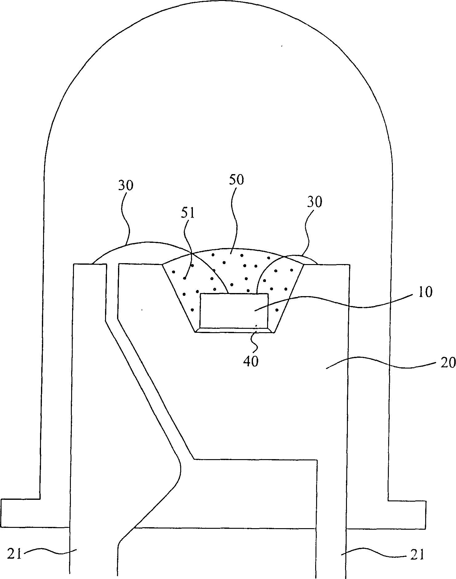
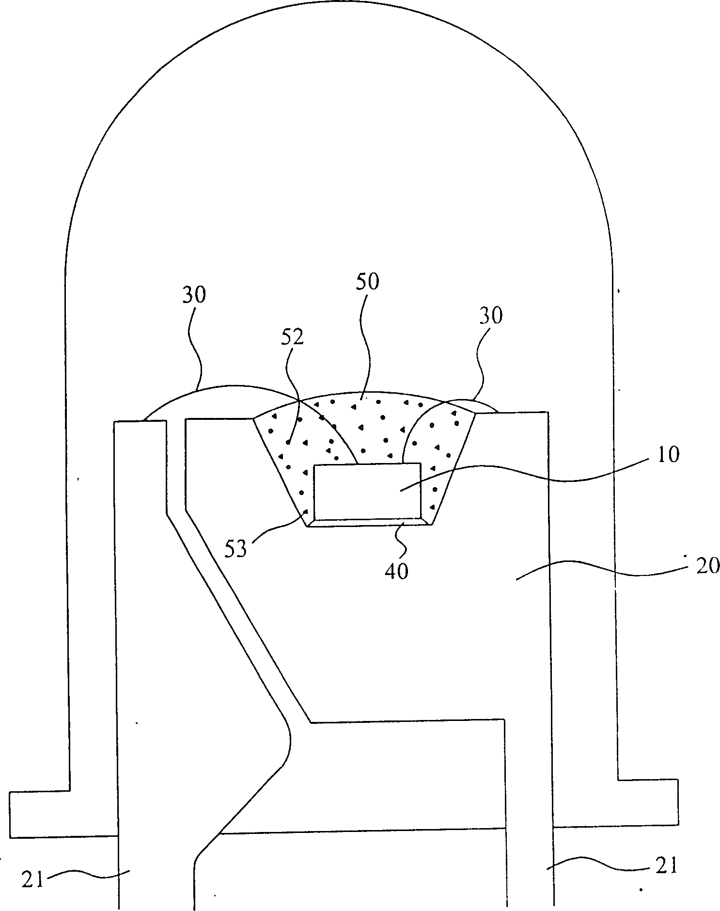
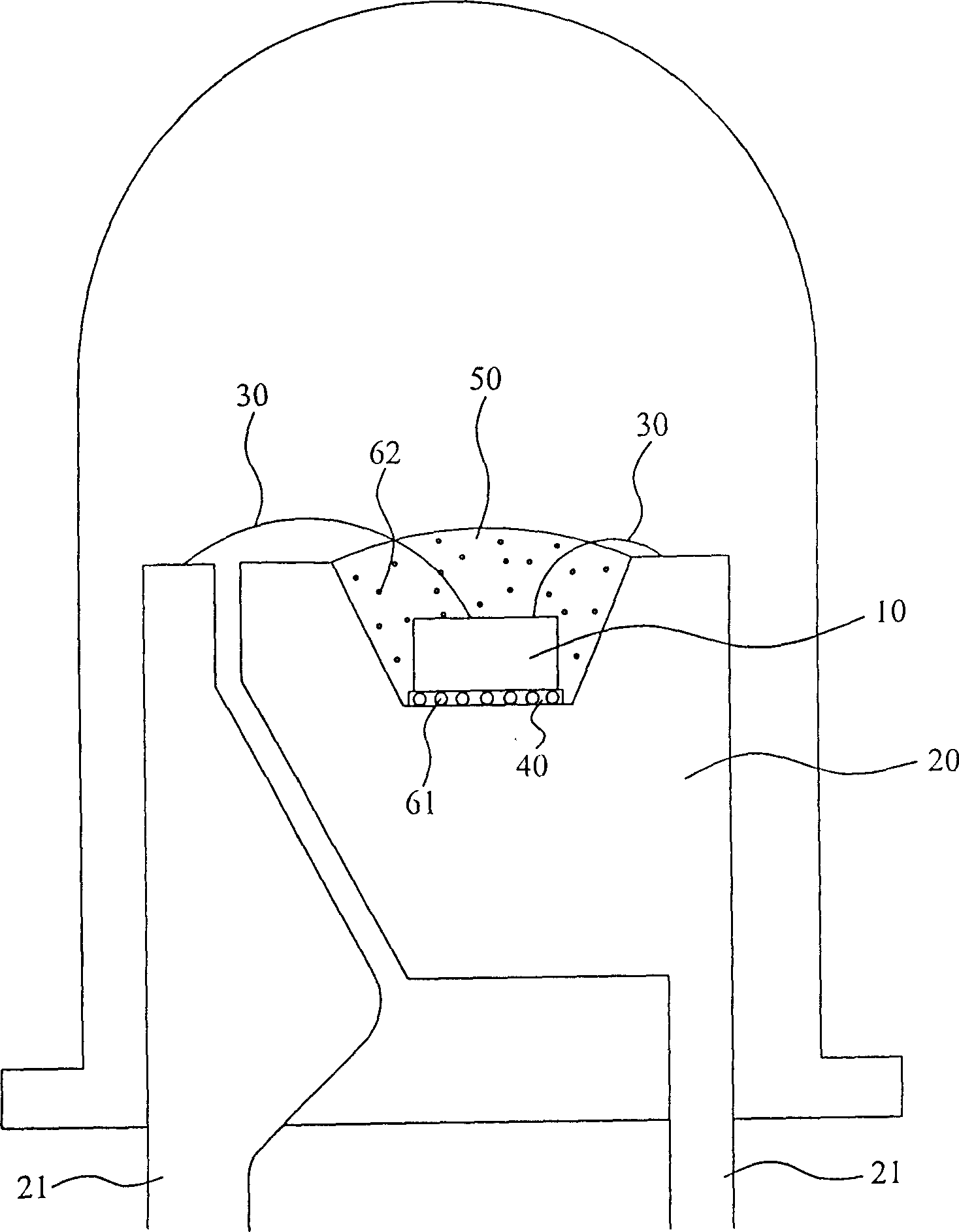
[0025] The "multi-wavelength light-emitting diode structure and its manufacturing process" of the present invention, the basic structure of the overall multi-wavelength light-emitting diode is as follows image 3 As shown, the light-emitting chip 10 is also fixed in a carrier 20 by using the crystal-bonding glue 40, and the connection between the light-emitting chip 10 and the electrode terminal 21 is formed by using the gold wire 30, and the light-emitting chip 10 is fixed by the fluorescent glue 50 having a fluorescent material. Covering is used to make the light source of the light-emitting chip excite the fluorescent material of the fluorescent glue 50 under the power-on effect of the light-emitting chip 10, so as to form a desired light color.
[0026] Among them, the overall multi-wavelength light-em...
PUM
 Abstract
Description
Claims
Application Information