High precision silicon slice bench and uses thereof

A silicon wafer table, high-precision technology, applied in electrical components, semiconductor/solid-state device manufacturing, circuits, etc., can solve the problem that the high-precision positioning of silicon wafers cannot be satisfied, the dynamic and static friction coefficients are difficult to keep the same, and affect the manufacturing accuracy of semiconductor equipment. and other problems, to achieve the effect of fast operation and response speed, low friction resistance, easy installation and replacement

Active Publication Date: 2006-11-22
SHANGHAI MICRO ELECTRONICS EQUIP (GRP) CO LTD +1
View PDF0 Cites 15 Cited by
  • Summary
  • Abstract
  • Description
  • Claims
  • Application Information

AI Technical Summary

Problems solved by technology

[0002] Most of the traditional silicon wafer stage structures use contact-type guide rail bases, which have large frictional resistance and high heat generation. It is difficult to keep the same dynamic and static friction coefficients. There will also be crawling
This traditional

Method used


Image

  • High precision silicon slice bench and uses thereof
  • High precision silicon slice bench and uses thereof
  • High precision silicon slice bench and uses thereof

Examples


Embodiment Construction

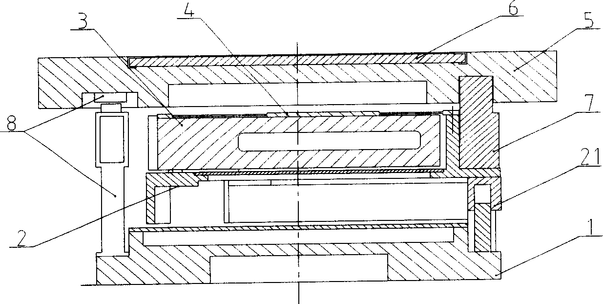
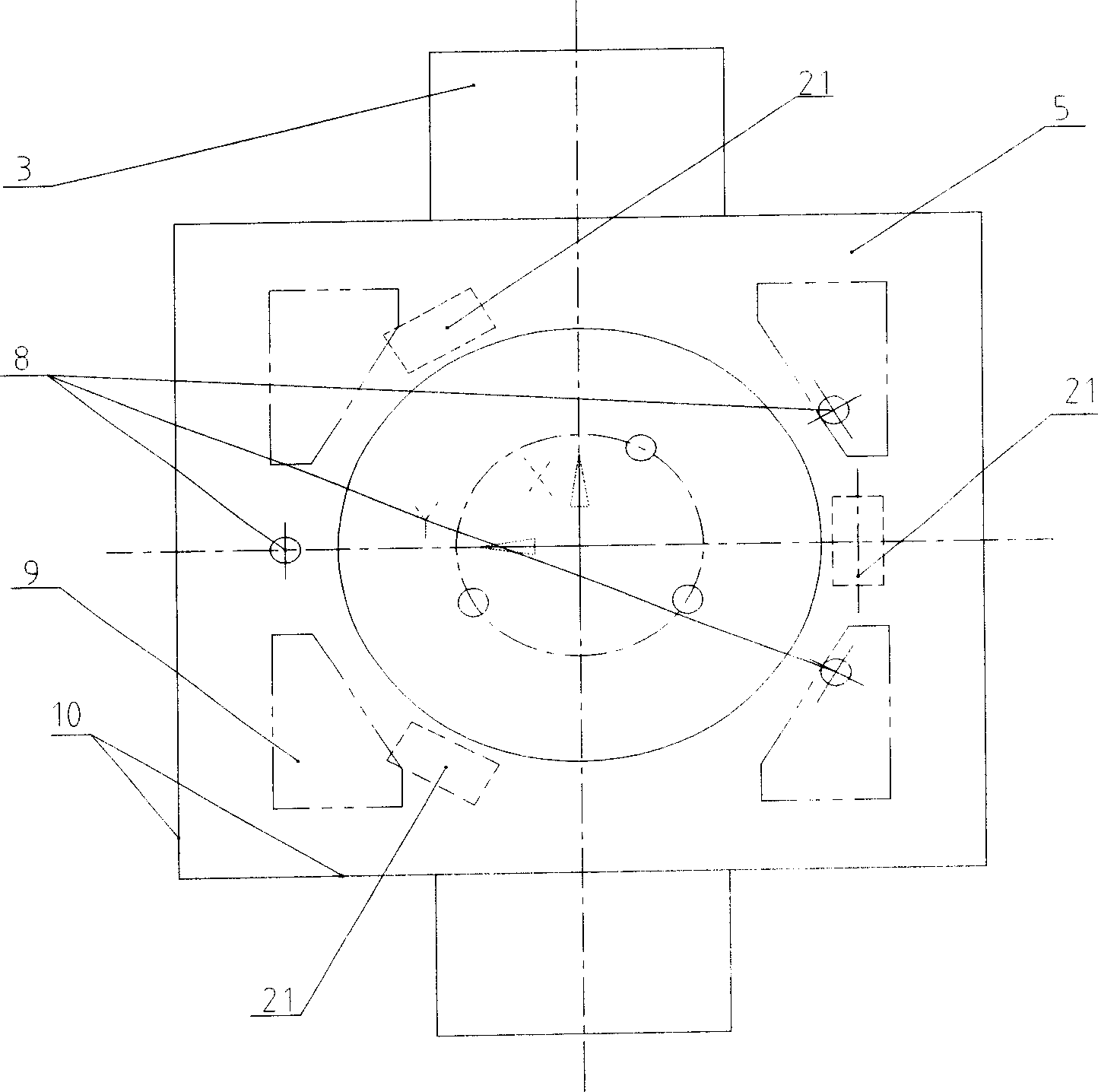
[0037] like figure 1 , 2 The shown high-precision silicon wafer stage includes an air-floating support 1, a leveling mechanism 2, a plane motor 3, and a reed 4, which are connected in sequence from bottom to top. Above the reed 4 is a square mirror 5. The upper surface is provided with a suction cup 6 for placing silicon wafers.

[0038] The invention uses the double-rigidity air-floating support 1 as the base to isolate the vibration of the frame, reduce the motion friction, eliminate the manufacturing error of the base platform, and ensure the speed stability of the scanning movement. In addition, it can prevent the shear pressure caused by the slight displacement caused by the overturning moment in the acceleration process to the air-bearing guide rail. In order to overcome the high-precision positioning of silicon wafers at high speed and high acceleration. The characteristics of the air flotation support 1 are: the motion friction resistance is extremely small, the cal...


PUM


Abstract

The invention discloses a high-precision silicon chip table and utility, which comprises the following parts: air-float support, leveling organization, plane motor and reed, wherein the square lens is set on the reed, which is supported by at least three square lens supports with bottom on the upper surface of leveling organization; the sucker is set on the upper surface of square lens to place silicon chip; the electric vortex sensor is set between air-float support and square lens; the leveling organization is composed of at least three leveling executers along circumferential direction, which correspond to square lens supports; the mirror plane is set on the square lens, which aligns mark board and reflects laser beam. The invention can assemble high-precise silicon chip within 50 nm vertical precision and 10 nm leveling precision, which improves manufacturing precision of semiconductor equipment greatly.

Description

technical field [0001] The invention relates to the field of semiconductor equipment manufacturing, and relates to a high-precision silicon wafer table and use thereof. Background technique [0002] Most of the traditional silicon wafer table structures use contact-type guide rail bases, which have large motion friction resistance, high heat generation, and it is difficult to keep the dynamic and static friction coefficients consistent. Crawling also occurs. This traditional silicon wafer stage structure can no longer meet the high-precision positioning problem of silicon wafers at high speed or high acceleration, which affects the manufacturing accuracy of semiconductor equipment to a large extent, and thus hinders the development of the semiconductor manufacturing industry. . SUMMARY OF THE INVENTION [0003] The purpose of the present invention is to provide a high-precision silicon wafer table and its application, which can enable the silicon wafer to have six degree...

Claims


Application Information

Patent Timeline
IPC IPC(8): H01L21/683H01L21/68
Inventor 齐芊枫李正贤
Owner SHANGHAI MICRO ELECTRONICS EQUIP (GRP) CO LTD
Why Eureka
Try Eureka