TV set and image display device

A technology for image display devices and televisions, applied in image/graphic display tubes, televisions, color televisions, etc.

Inactive Publication Date: 2006-12-20
CANON KK
View PDF3 Cites 3 Cited by
  • Summary
  • Abstract
  • Description
  • Claims
  • Application Information

AI Technical Summary

Problems solved by technology

One of the problems is that an additional light source must be added to the display device in order to illuminate the liquid crystal plane, since th

Method used


Image

  • TV set and image display device
  • TV set and image display device
  • TV set and image display device

Examples


example 1

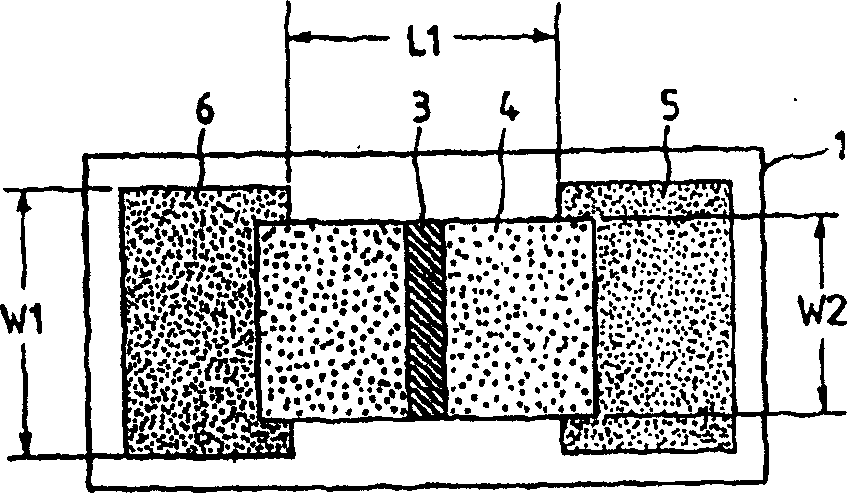
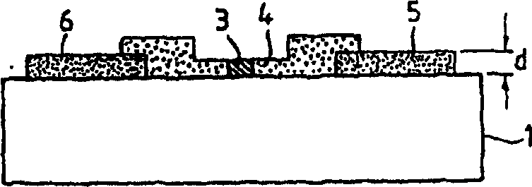
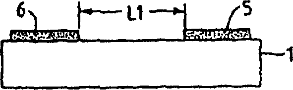
[0132] Example 1. The basic structure of the device used in this example and Figure 1A floor plan and Figure 1B The same as shown in the (section) figure. Four identical devices are formed on a substrate 1 . Notice Figure 11 The meaning of the labels in and Figure 1A , 1B The same reference numerals represent the same elements.

[0133] The method of making this device and Figures 2A to 2C The method of explanation is basically the same.

[0134] Refer below Figure 1A , 1B and Figures 2A to 2C The basic structure of the device and its fabrication method are described.

[0135] see Figure 1A Figure 1B , The sample of the prepared electron-emitting device includes a substrate 1, a pair of device electrodes 5, 6, and a thin film 4 including an electron-emitting region 3.

[0136] see Figure 1A , 1B and 2A to 2C, the method of fabricating the device based on the experiments performed on this sample is described as follows:

[0137] Step A:

[0138] After...

example 2

[0159] In this example, a large number of surface conduction electron-emitting devices are arranged in a simple matrix to form an image forming apparatus.

[0160] Figure 13 is a partially enlarged plan view of the electron source substrate of the device. Figure 14 yes Figure 13The enlarged schematic diagram of the cross section of the substrate along the A-A line. pay attention to Figure 13 , 14 , 15A to 15D and 16E to 16H the same reference numerals represent the same elements. In this way, reference numerals 81, 82, and 83 respectively represent the substrate, the X-direction wiring corresponding to the external terminal DXm (also called the lower wiring), and the y-directional wiring corresponding to the external terminal Dyn (also called the upper wiring). ), and the reference numeral 4 represents the thin film comprising the electron emission region, the reference numerals 5 and 6 represent a pair of device electrodes, and the reference numerals 141 and 142 repr...

example 3

[0195] Samples of electron-emitting devices were prepared as described in Example 1.

[0196] Each electron-emitting device produced had a device width W2 of 300 μm, a thin film 2 for the electron-emitting region of the device had a thickness of 10 nm, and a resistance per unit area of ​​5×10 4 Ω / port. In addition, the device used was the same as the corresponding device in Example 1.

[0197] then press image 3 A dosing system is positioned as shown and evacuated from the inside using a magnetic levitation pump up to 2×10 -8 Torr vacuum. Next, a voltage is applied to the device electrodes 5 and 6 using a power source 31 that supplies a device voltage Vf to the device, and the device is subjected to electric forming (electric forming treatment). Figure 4B The voltage waveforms used for the electroforming process are shown in .

[0198] exist Figure 4B Among them, T1 and T2 respectively represent the pulse width and pulse interval of the applied pulse voltage, which ar...


PUM

PropertyMeasurementUnit
Film thicknessaaaaaaaaaa
Thicknessaaaaaaaaaa

Abstract

The present invention relates to a TV set and picture display device. Said TV set comprises: (A) a display panel that includes a plurality of electron emitting parts and a screen used for displaying pictures by electron radiation. Each said electron emitting device comprises: electrode pairs; electric membrane, including a crack and composed of electric materials but carbon and disposed between the said electrodes and connected to them; and a carbonic deposit with carbon as its main component. The said carbonic group deposit is disposed in the crack and connected to the electric membrane, and it has space formed wherein, which is narrow than the crack. (B) A TV signal receiving circuit used for receiving TV signals and (C) a drive circuit used for displaying pictures according to the TV signal onto the screen.

Description

[0001] This application is a divisional application of the patent application with the filing date of June 24, 1994, the application number of 200410003954.4, and the title of the invention "Manufacturing method of electron emission device". technical field [0002] The invention relates to a television and an image display device. Background technique [0003] Known electron-emitting devices are of two types, ie, thermionic type and cold cathode type. Among them, the cold cathode type includes field emission type (hereinafter referred to as FE type), metal / insulator / metal type (hereinafter referred to as MIM type) and surface conduction type. [0004] Examples of FE electron-emitting devices are in W.P.Dyke and W.W.Dolan, "Fieldemission", Advance in Electron Pnysics, 8, 89 (1956) and C.A.spindt, "PHYSICAL properties of thin-filmfieldemission Cathodes with molybdenum cones", J.Appl.phys ., 47, 5284 (1976). [0005] MIM devices are described in C. A. Mead, "The tunnel-emiss...

Claims


Application Information

Patent Timeline
IPC IPC(8): H04N5/44H04N3/16H01J31/12H01J9/02
CPCH01J2201/3165
Inventor 大西敏一山野边正人野村一郎鲈英俊坂野嘉和小野武夫三留正则
Owner CANON KK
Why Eureka
Try Eureka