Strong magnetic filed Hall effect testing apparatus and testing method thereof
A Hall effect and testing device technology, applied in the field of testing, can solve the problems of error-prone, low efficiency and poor reliability of manual data processing, etc.
- Summary
- Abstract
- Description
- Claims
- Application Information
AI Technical Summary
Problems solved by technology
Method used
Image

Examples
Embodiment Construction
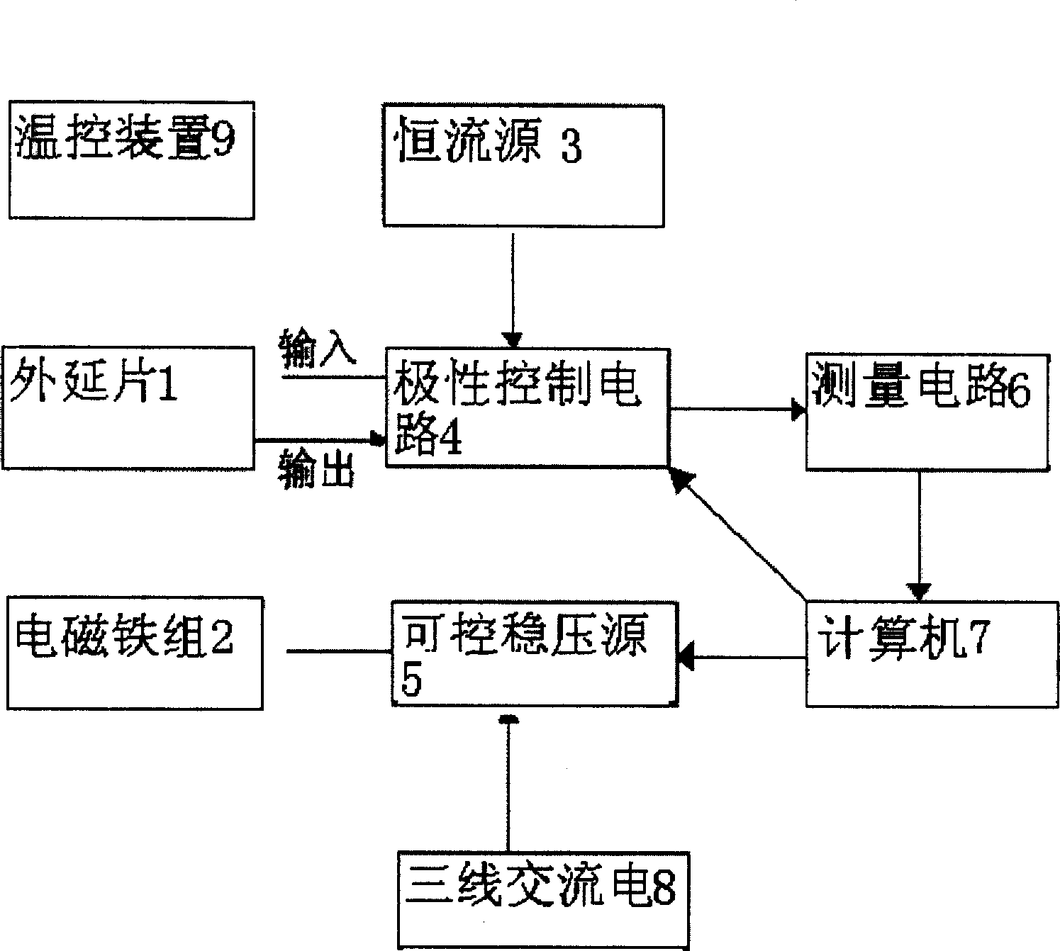
[0024] Depend on figure 1 It can be seen that the Hall effect testing device of a kind of strong magnetic field of the present invention consists of epitaxial wafer 1, electromagnet group 2, constant current source 3, polarity control circuit 4, controllable voltage regulator source 5, measurement circuit 6, Computer 7, three-phase alternating current 8, temperature control device 9 etc. are connected to form. Concrete line connection: the output control line of the computer 7 is connected with the polarity control circuit 4 and the controllable voltage source 5 respectively; the output line of the measurement circuit 6 is connected with the input control line of the computer 7; the output line of the constant current source 3 is connected with the pole The input line of polarity control circuit 4 is connected; the input and output lines of epitaxial wafer 1 are respectively connected with the output and input control lines of polarity control circuit 4; the output line of co...
PUM
 Abstract
Description
Claims
Application Information
 - R&D
- Intellectual Property
- Life Sciences
- Materials
- Tech Scout
- Unparalleled Data Quality
- Higher Quality Content
- 60% Fewer Hallucinations
Browse by: Latest US Patents, China's latest patents, Technical Efficacy Thesaurus, Application Domain, Technology Topic, Popular Technical Reports.
© 2025 PatSnap. All rights reserved.Legal|Privacy policy|Modern Slavery Act Transparency Statement|Sitemap|About US| Contact US: help@patsnap.com