

Multi-bus automobile communication control module based on TCN
A vehicle communication and control module technology, applied in bus network, railway signal and safety, data exchange through path configuration, etc., can solve the problems of large volume, large volume, small storage space, etc., and achieve large storage space and equipment volume Small, easily programmable effects
- Summary
- Abstract
- Description
- Claims
- Application Information
AI Technical Summary
Problems solved by technology
Method used
Image

Examples
Embodiment Construction
[0009] Below in conjunction with accompanying drawing and embodiment the present invention will be further described:
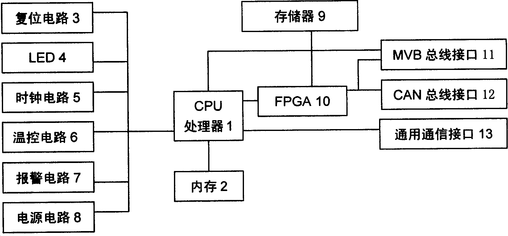
[0010] refer to figure 1 , the present invention includes a CPU processor 1, a memory 2 electrically connected to the CPU processor 1, a reset circuit 3, an LED 4, a clock circuit 5, a temperature control circuit 6, an alarm circuit 7, and a power supply circuit 8, and the CPU processor 1 also Connect with FPGA10, described FPGA10 is connected with memory 9, CAN bus interface 12, MVB bus interface 11, and described MVB bus interface 11 is also directly connected with CPU processor 1, and CPU processor 1 is also connected with general communication interface 13.
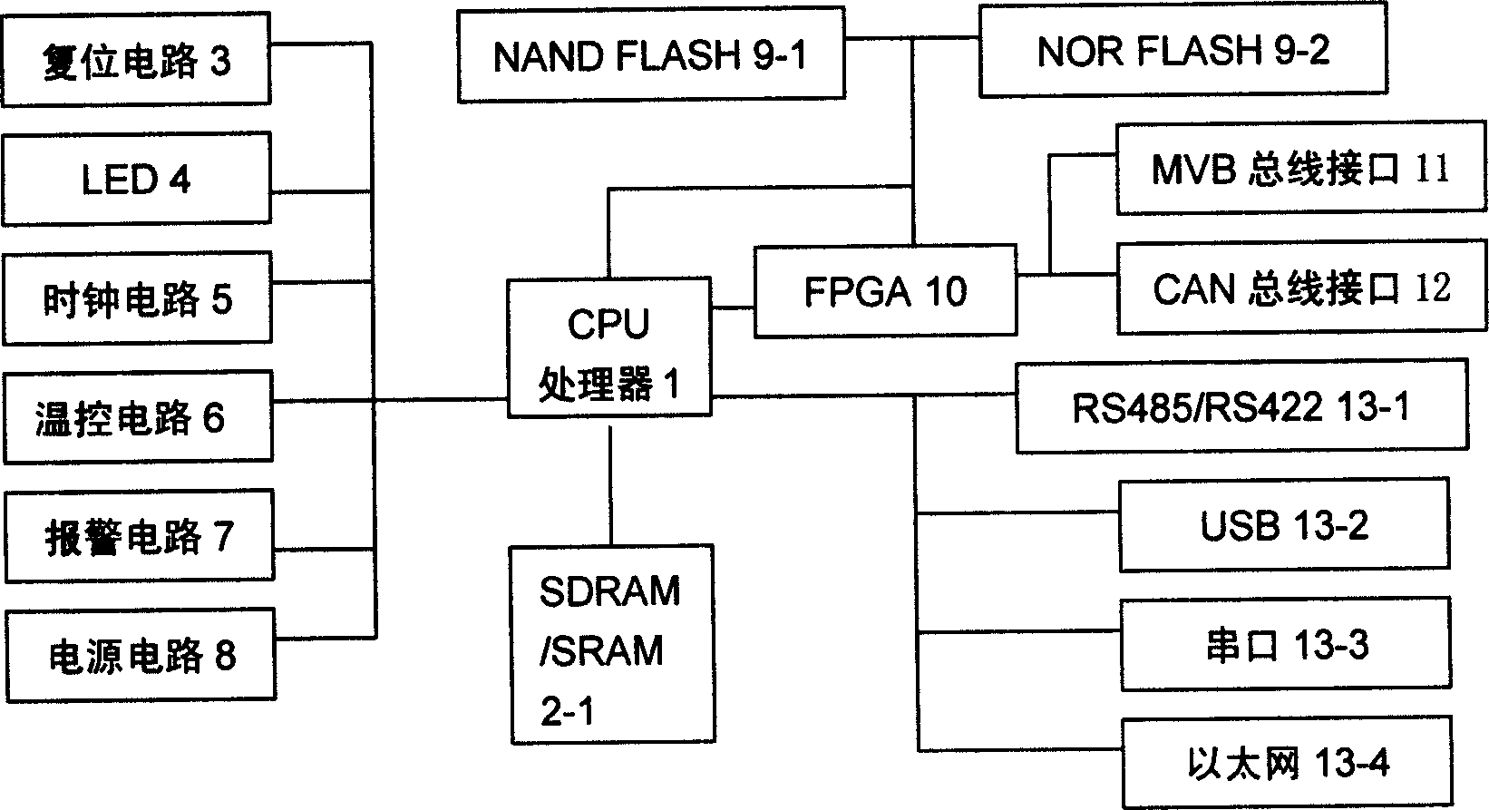
[0011] refer to figure 2 , the present embodiment is connected with reset circuit 3, LED4, clock circuit 5, temperature control circuit 6, alarm circuit 7, power supply circuit 8 on CPU processor 1, and the memory 2 that is connected with CPU processor 1 is SDRAM or SRAM2-1 The memory 9 connected ...
PUM
 Abstract
Description
Claims
Application Information