Thin film transistor, display, liquid crystal display, and method of manufacturing them

A technology for thin film transistors and display devices, which is used in the fields of display devices, wiring, and thin film transistors, and can solve problems such as inability to handle the surface of display panels.

Inactive Publication Date: 2007-01-03
SEMICON ENERGY LAB CO LTD
View PDF2 Cites 17 Cited by
  • Summary
  • Abstract
  • Description
  • Claims
  • Application Information

AI Technical Summary

Problems solved by technology

But as the size of the substrate increases, the entire surface of the display panel cannot be processed by means of a single exposure

Method used


Image

  • Thin film transistor, display, liquid crystal display, and method of manufacturing them
  • Thin film transistor, display, liquid crystal display, and method of manufacturing them
  • Thin film transistor, display, liquid crystal display, and method of manufacturing them

Examples


Embodiment Construction

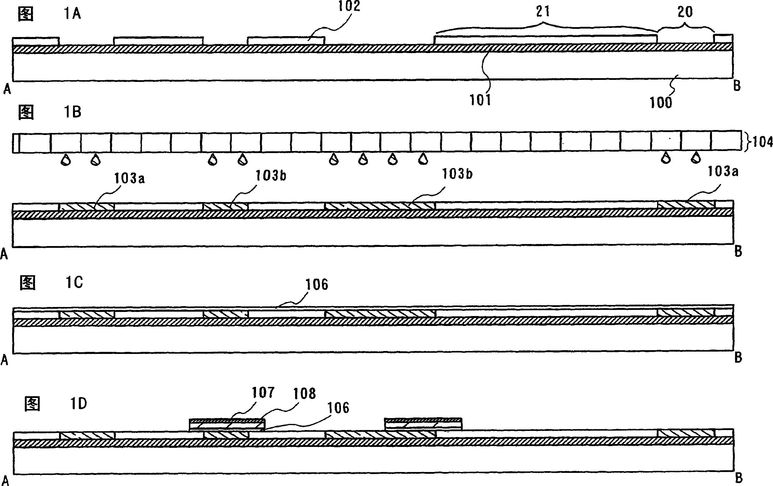
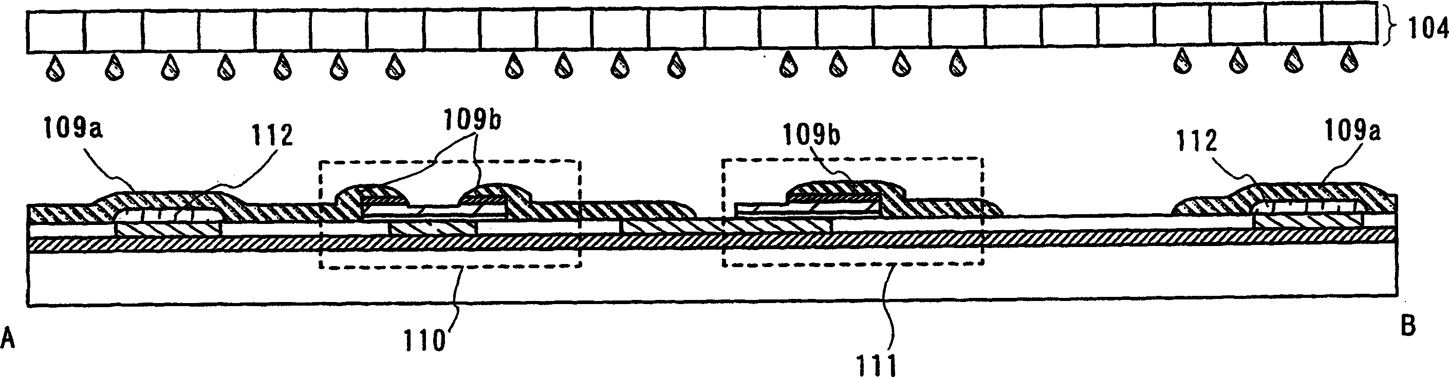
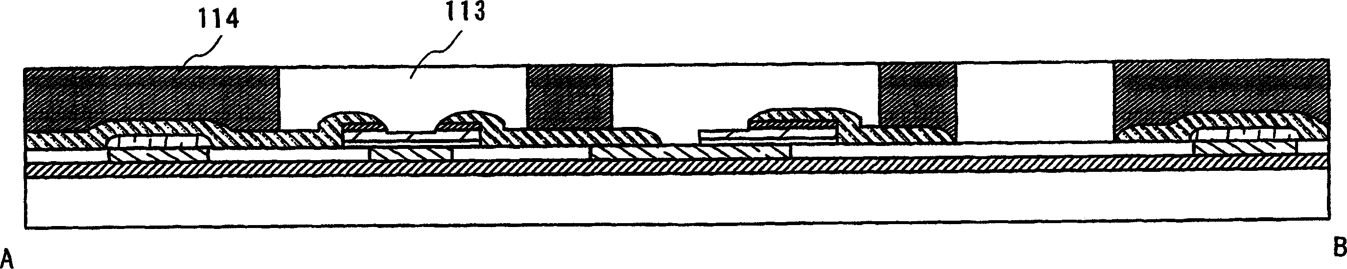
[0118] Embodiments of the present invention are described in detail below with reference to the accompanying drawings. Note that it can be easily understood by those skilled in the art that the present invention is not limited to the following description, and various changes in form and details can be made without departing from the spirit and scope of the present invention. Therefore, the present invention should not be limited to the description of each embodiment mode below. In the respective drawings for explaining the respective embodiment modes, the same reference numerals are given to the same components, and descriptions thereof will not be repeated.

[0119] A TFT has 3 terminals, namely a gate, a source, and a drain; but a source terminal (source electrode) and a drain terminal (drain electrode) cannot be clearly distinguished due to the structure of the transistor. Therefore, when describing connections between elements, one of the source electrode and the drain e...


PUM

PropertyMeasurementUnit
widthaaaaaaaaaa
depthaaaaaaaaaa
depthaaaaaaaaaa

Abstract

As a wiring becomes thicker, discontinuity of an insulating film covering the wiring has become a problem. It is difficult to form a wiring with width thin enough for a thin film transistor used for a current high definition display device. As a wiring is made thinner, signal delay due to wiring resistance has become a problem. In view of the above problems, the invention provides a structure in which a conductive film is formed in a hole of an insulating film, and the surfaces of the conductive film and the insulating film are flat. As a result, discontinuity of thin films covering a conductive film and an insulating film can be prevented. A wiring can be made thinner by controlling the width of the hole. Further, a wiring can be made thicker by controlling the depth of the hole.

Description

technical field [0001] The present invention relates to methods of fabricating wiring, thin film transistors, and display devices, each employing a method whereby patterns can be selectively formed. More specifically, the present invention relates to a display device having components such as transistors formed on a large glass substrate using a droplet discharge method typically an inkjet method as a method capable of selectively forming patterns. The active element, the invention also relates to a manufacturing method of a display device. Furthermore, the present invention relates to a wiring, a thin film transistor, and a display device formed by a method capable of selectively forming patterns. Background technique [0002] By patterning various thin films using an exposure process using a photomask and a manufacturing technique of a semiconductor integrated circuit, so-called thin film transistors (hereinafter also referred to as "TFTs") on a glass substrate have been ...

Claims


Application Information

Patent Timeline
Patent Type & Authority Applications(China)
IPC IPC(8): H01L21/336G02F1/1368G09F9/30H01L21/288H01L21/3205H01L29/786
Inventor 山崎舜平前川慎志神野洋平
Owner SEMICON ENERGY LAB CO LTD
Why Eureka
Try Eureka