Unlock instant, AI-driven research and patent intelligence for your innovation.

Integrated circuit device and electronic instrument

A technology of integrated circuits and circuit blocks, which is applied in the direction of circuits, electrical components, and electrical solid devices, and can solve the problems of fixed display panel size and difficulty in installation, and achieve the effects of easy adjustment, reduced layout area, and increased layout area

Active Publication Date: 2007-01-10
SEIKO EPSON CORP
View PDF1 Cites 3 Cited by
  • Summary
  • Abstract
  • Description
  • Claims
  • Application Information

AI Technical Summary

Problems solved by technology

[0003] However, the size of the display panel incorporated into a mobile phone etc. is almost fixed
Therefore, if a fine process is used to simply shorten the integrated circuit device of the display driver and reduce the size of the integrated circuit substrate, it will lead to problems such as difficulty in installation.

Method used


Image

  • Integrated circuit device and electronic instrument
  • Integrated circuit device and electronic instrument
  • Integrated circuit device and electronic instrument

Examples


Embodiment Construction

[0061] Hereinafter, a preferred embodiment of the present invention will be described in detail. The embodiments described below do not improperly limit the content of the present invention described in the claims, and all the configurations described in the embodiments are not essential requirements for the present invention.

[0062] 1. Comparative example

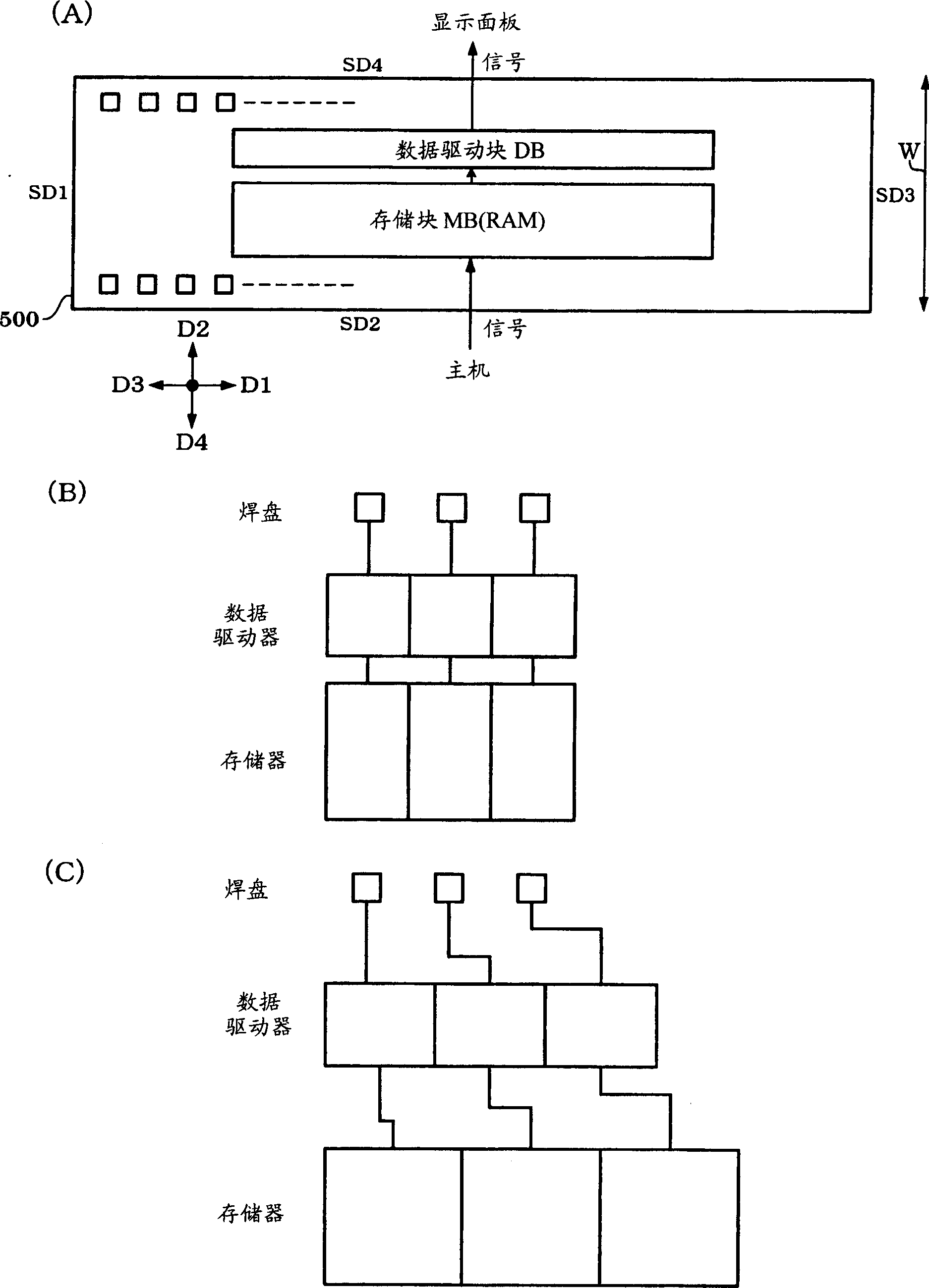
[0063] in figure 1 In (A), an integrated circuit device 500 as a comparative example of this embodiment is shown. figure 1 The integrated circuit device 500 of (A) includes a memory block MB (display data RAM) and a data drive block DB. In addition, the memory block MB and the data drive block DB are arranged along the D2 direction. In addition, the memory block MB and the data driving block DB form an ultra-flat block whose length in the D1 direction is longer than the width in the D2 direction.

[0064] The image data from the host side is written into the memory block MB. In addition, the data driving block DB converts ...


PUM


Abstract

The invention provides a slim, thin and long integrated circuit device, and electronic equipment incorporating the same. The integrated circuit device includes a pad PDx and an electrostatic discharge protection element ESDx formed in a rectangular region and electrically connected with the pad PDx. The pad PDx is disposed in an upper layer of the electrostatic discharge protection element ESDx so that an arrangement direction of the pads is parallel to a long side direction of the region in which the electrostatic discharge protection element ESDx is formed, and the pad PDx overlaps part or the entirety of the electrostatic discharge protection element ESDx.

Description

Technical field [0001] The invention relates to an integrated circuit device and electronic equipment. Background technique [0002] As an integrated circuit device that drives a display panel such as a liquid crystal panel, there is a display driver (LCD driver). In this display driver, it is necessary to reduce the size of the integrated circuit substrate in order to reduce the cost. [0003] However, the size of the display panel incorporated in a mobile phone or the like is almost fixed. Therefore, if a fine process is used to simply shorten the integrated circuit device of the display driver and reduce the size of the integrated circuit substrate, it will cause problems such as difficulty in mounting. [0004] Patent Document 1: JP 2001-222249 A Summary of the invention [0005] The present invention was made in view of the above-mentioned technical problems, and its object is to provide a slim and elongated integrated circuit device and an electronic device including the s...

Claims


Application Information

Patent Timeline
IPC IPC(8): H01L27/00G09G3/20G09G3/36G09G5/36G09G5/39
Inventor 熊谷敬石山久展前川和广伊藤悟藤濑隆史唐泽纯一小平觉齐木隆行高宫浩之
Owner SEIKO EPSON CORP
Features
  • R&D
  • Intellectual Property
  • Life Sciences
  • Materials
  • Tech Scout
  • Unparalleled Data Quality
  • Higher Quality Content
  • 60% Fewer Hallucinations
Learn More