
Semiconductor laser unit and optical pickup device

一种半导体、激光的技术,应用在半导体激光器、半导体器件、激光器等方向,能够解决困难、半导体激光单元制造工序复杂、粉尘污染等问题,达到实现特性安定、小型化可信度、容易组装的效果

Inactive Publication Date: 2007-01-10
PANASONIC CORP
View PDF3 Cites 0 Cited by
  • Summary
  • Abstract
  • Description
  • Claims
  • Application Information

AI Technical Summary

Problems solved by technology

[0018] However, in the structure of the semiconductor laser unit described in Patent Document 2, it is difficult to achieve both miniaturization and high performance.
[0019] In addition, in the optical head device described in Patent Document 3, thinning becomes difficult because the flexible substrate protrudes from the board surface.
In addition, the optical head device may be polluted by dust generated when the shells are joined.
[0020] In addition, the manufacturing process of the semiconductor laser unit described in Patent Document 4 is complicated, and it is difficult to shorten the working time, and it is also difficult to sufficiently ensure the installation accuracy of each component.
In addition, in the semiconductor laser unit described in Patent Document 4, since the terminal portion of the flexible substrate is attached to the metal island in a bent state, the work at the time of manufacture becomes complicated, and there is a possibility that the connection portion may be damaged. Insufficient bond strength

Method used


Image

  • Semiconductor laser unit and optical pickup device
  • Semiconductor laser unit and optical pickup device
  • Semiconductor laser unit and optical pickup device

Examples


no. 1 approach

[0065] First, a semiconductor laser unit according to a first embodiment of the present invention will be described with reference to FIGS. 1 and 2 .

[0066] Figure 1(a) to Figure 1(c) , is a perspective view illustrating a method of manufacturing the semiconductor laser unit according to the first embodiment of the present invention. Fig. 2(a) is a top view showing the semiconductor laser unit according to the first embodiment. Fig. 2(b) is a side view showing the semiconductor laser unit according to the first embodiment.

[0067] The semiconductor laser unit of this embodiment has a simple structure that is easy to assemble, and it is easy to dissipate heat, and achieve high performance and miniaturization.

[0068] The semiconductor laser unit of this embodiment is assembled as follows.

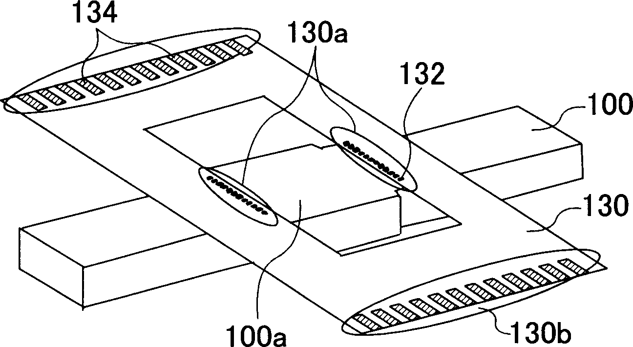
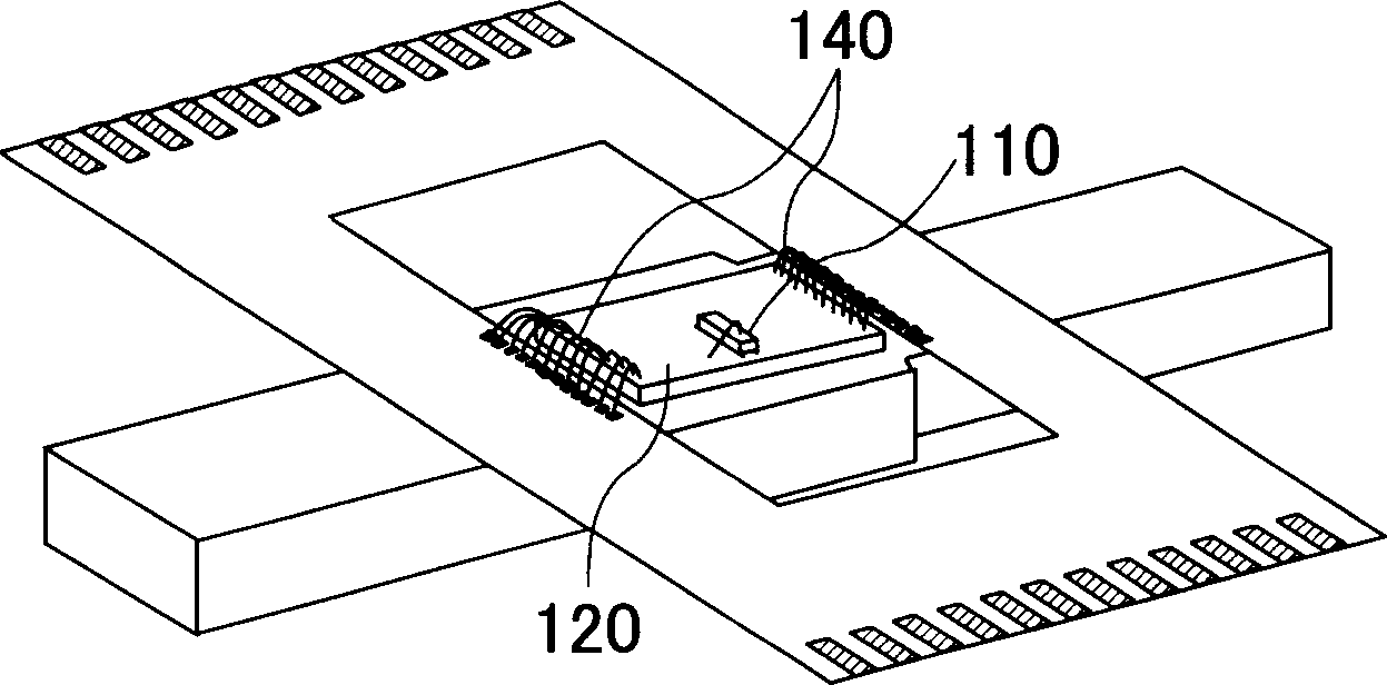
[0069] First, as shown in FIG. 1( a ), a metal plate 100 made of copper or the like is prepared, and a flexible substrate 130 in which an opening is provided in the center is prepared...

no. 2 approach

[0097] Next, an optical pickup device according to a second embodiment of the present invention will be described with reference to FIG. 5 .

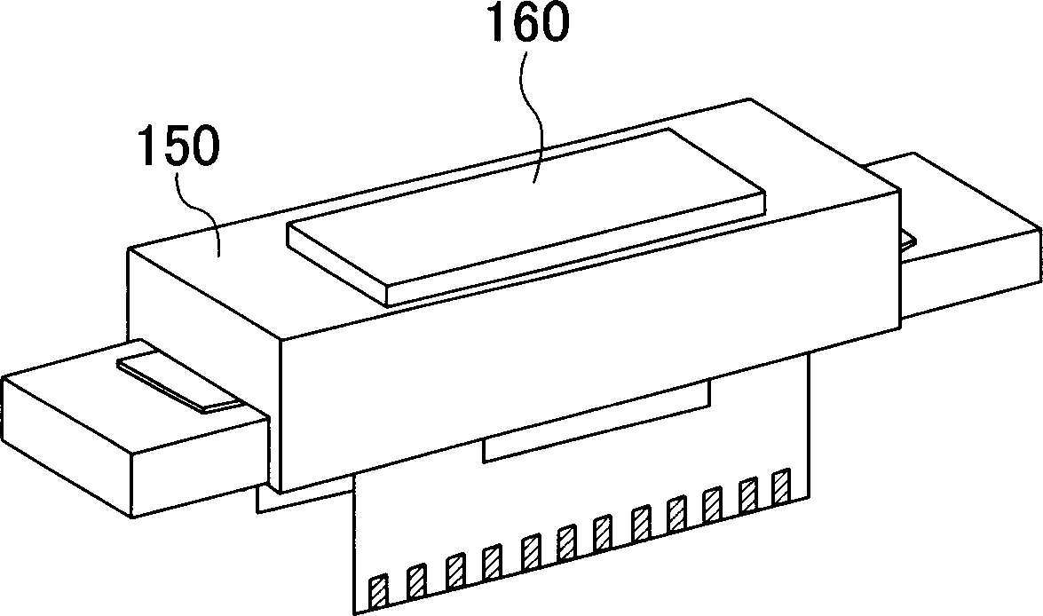
[0098] FIG. 5(a) is a top view of the optical pickup device 500 of this embodiment. FIG. 5( b ) is a cross-sectional view of the optical pickup device 500 .

[0099] The optical pick-up device 500 of the present embodiment comprises: collimator 510; Mirror 520; Objective lens 530; The semiconductor laser unit 540 involved in the first embodiment; The heat release block 550 is bonded and fixed with a silicon-based thermally conductive adhesive. The laser light emitted from the semiconductor laser unit 540 irradiates the optical disc 570 through the collimating mirror 510 , the reflecting mirror 520 , and the objective lens 530 . The reflected light reflected from the optical disc 570 enters the semiconductor laser unit through the same optical path.

[0100] The wiring connection between the outside of the flexible substrate of the se...


PUM


Abstract

The semiconductor laser unit includes: a metal plate having a center portion wider than the remaining portions; a flexible substrate having a first opening; a substrate mounted on the center portion; a semiconductor laser placed on the substrate; a frame having a second opening and fixing the flexible substrate in the state of being bent along from the top surface to both side faces of the metal plate; and an optical element covering the second opening. The flexible substrate is fixed so that the first opening extends over the top surface and both side faces of the center portion.

Description

technical field [0001] The present invention relates to a semiconductor laser unit, in particular to a semiconductor laser constituting an optical pick-up device for writing / reading information to an optical disk, such as a digital versatile disk (DVD) or a compact disk (CD). unit and the optical pick-up device containing it. Background technique [0002] In recent years, not only music information but also video information recording media, such as compact disk (CD) type (CD-ROM, CD-R, CD-RW, etc.) and digital versatile disk (DVD) type (DVD-ROM , DVD-RW, DVD-RAM, etc.) recording media are rapidly spreading. At the same time, optical disk drives for writing information to / from such recording media and reading written information are rapidly spreading. On the optical pickup device that becomes the heart of the optical disc drive, it is necessary to support high-speed output for high-magnification recording, and to support both high-density discs (CD) and digital versatile d...

Claims


Application Information

Patent Timeline
Patent Type & Authority Applications(China)
IPC IPC(8): H01S5/022H01L23/02G11B7/125
CPCG11B7/127H01S5/02248H01L2224/48091H01S5/02325H01L2924/00014H01S5/026
Inventor 富士原洁立柳昌哉冈本重树
Owner PANASONIC CORP
Learn More