

Adhesive sheet, dicing tape-integrated adhesive sheet, film, method for manufacturing semiconductor device, and semiconductor device
A bonding sheet, semiconductor technology, applied in the direction of semiconductor/solid device manufacturing, semiconductor device, film/sheet adhesive, etc., can solve the problem of large amount of silver paste protruding, hindering chip miniaturization, and silver paste spreading And other issues
- Summary
- Abstract
- Description
- Claims
- Application Information
AI Technical Summary
Problems solved by technology
Method used
Image

Examples
Embodiment approach 1
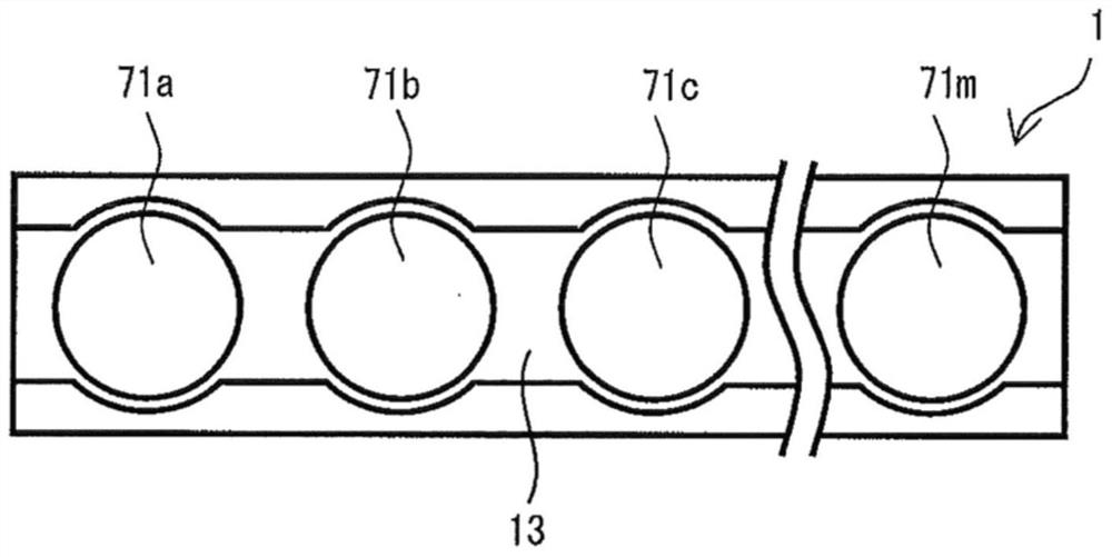
[0076] (Film 1)
[0077] Such as figure 1 with figure 2 As shown, the film 1 includes a separator 13 and an adhesive sheet 11 arranged on the separator 13 . More specifically, the film 1 includes a separator 13 and dicing tape-integrated adhesive sheets 71 a , 71 b , 71 c , . The distance between the dicing tape-integrated adhesive sheet 71a and the dicing tape-integrated adhesive sheet 71b, the distance between the dicing tape-integrated adhesive sheet 71b and the dicing tape-integrated adhesive sheet 71c, ... the dicing tape-integrated adhesive sheet The distance between the adhesive sheet 71l and the dicing tape integrated adhesive sheet 71m is constant. The film 1 can be formed into a roll.
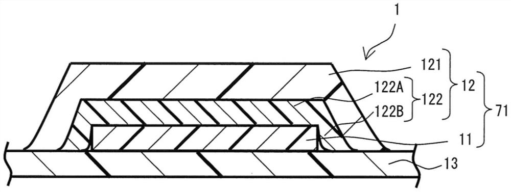
[0078] The dicing tape-integrated adhesive sheet 71 includes the dicing tape 12 and the adhesive sheet 11 arranged on the dicing tape 12 . The dicing tape 12 includes a base material 121 and an adhesive layer 122 arranged on the base material 121 . The adhesive sheet 11 can ha...
Deformed example 1
[0200] The contact portion 122A of the adhesive layer 122 has a property of being cured by radiation. The peripheral portion 122B of the adhesive layer 122 also has a property of being cured by radiation. In the manufacturing method of the semiconductor device, the chip 5 for die bonding is formed, the adhesive layer 122 is irradiated with ultraviolet rays, and the chip 5 for die bonding is picked up. Thereby, since the adhesive force of the adhesive layer 122 with respect to the chip|tip 5 for die bonding falls, it becomes possible to pick up the chip|tip 5 for die bonding easily.
Deformed example 2
[0202] The contact portion 122A of the adhesive layer 122 is cured by radiation. The peripheral portion 122B of the adhesive layer 122 is also cured by radiation.
PUM
| Property | Measurement | Unit |
|---|---|---|
| glass transition temperature | aaaaa | aaaaa |
| particle size | aaaaa | aaaaa |
| epoxy equivalent | aaaaa | aaaaa |
Abstract
Description
Claims
Application Information