

Organic electroluminescent element and its manufacturing method
An electroluminescent device and electroluminescent technology, which can be used in the manufacture of semiconductor/solid-state devices, electric solid-state devices, electrical components, etc., and can solve problems such as insufficient durability.
- Summary
- Abstract
- Description
- Claims
- Application Information
AI Technical Summary
Problems solved by technology
Method used
Image

Examples
Embodiment approach 1
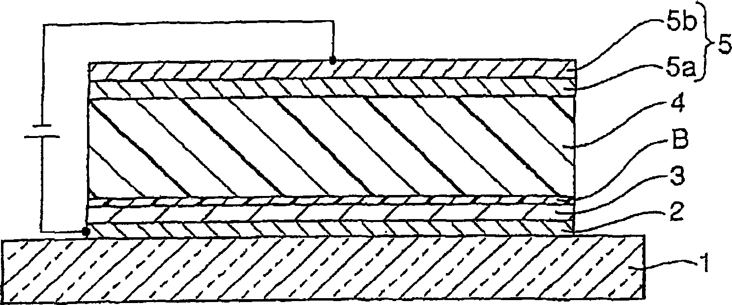
[0076] figure 1 It is a schematic diagram of a polymer organic EL device according to an embodiment of the present invention.
[0077] The present embodiment is characterized in that a metal oxide thin film is formed on the transparent anode 2 on the light-transmitting substrate 1 as the charge injection layer 3, and a polymer material layer as the buffer layer B having an electron blocking function and a polymer material layer as the buffer layer B having an electron blocking function are laminated thereon. Another polymer material layer of the light-emitting layer 4, the cathode 5 is formed above all of them.
[0078] That is, if figure 1 As shown, the organic electroluminescence device of the embodiment is made of a substrate 1 made of a transparent glass material, an ITO layer (indium titanium oxide) formed on the substrate 1 as the anode 2, and a charge injection layer 3 formed thereon. The metal oxide film is composed of an electron blocking layer made of a polymer mat...
Embodiment 1
[0086] Next, embodiments of the present invention are described.
[0087] structure and figure 1 given the same structure and will refer to figure 1 do explain.
[0088] The organic electroluminescent device of embodiment 1 is made by the substrate 1 that is called Corning 7029# 1mm thick glass sheet, is formed on it and is formed on the anode 2 that is made of 20nm thick ITO thin film, is formed on the anode 2 and is made of 20nm A charge injection layer 3 composed of a thick molybdenum oxide film, a polyfluorene-based compound formed on the charge injection layer 3 (especially poly[9,9-dioctylfluorene-2,7-diyl]-alternating-co- (N, N'-diphenyl)-N, N'-two (p-butyl-oxyphenyl)-1,4-diaminobenzene) (poly[9,9-dioctylfluorenyl-2,7-diyl ]-alt-co-(N,N′-diphenyl)-N,N′-di(p-butyl-oxyphenyl)-1,4-diaminobenzene) 20nm thick buffer layer B, made of polyfluorene-based compound ( Especially poly[(9,9-dioctylfluorene-2,7-diyl)-co-1,4-benzo-{2,1'-3}-thiadiazole] (poly[(9, 9-dioctylfluoreny...
Embodiment 2
[0129] Next, Embodiment 2 of the present invention will be discussed.
[0130] In the above Example 1, the polyfluorene-based compound was used in the light-emitting layer, but this example uses a PPV-based material in the light-emitting layer 4, poly[2-methoxy-5-(2-ethylhexyloxy base)-1,4-phenylenevinylene](poly[2-methoxy-5-(2-ethylhexyloxy)-1,4-phenylenevinylene]). Like Example 1, this material is also commercially available from Nihon SiberHegner K.K.
[0131] Other structures are constituted the same as in Embodiment 1.
[0132] In this case, the luminous intensity can generally be increased further.
[0133] In addition, in Example 1 and Example 2, a glass substrate was used as the substrate 1, but it is not limited to glass. Usually glass is used. Also in this embodiment, a glass substrate is used. Various materials have been suggested as the substrate material, including glass, plastic film, and the like, and these can be used as the substrate 1 of the present inve...
PUM
 Abstract
Description
Claims
Application Information