

Array substrate for display device
An array substrate and substrate technology, which is applied in the field of display devices, can solve the problems of increasing capacitance, changing pixel voltage and brightness, etc., and achieves the effects of eliminating etching and reducing contact resistance.
- Summary
- Abstract
- Description
- Claims
- Application Information
AI Technical Summary
Problems solved by technology
Method used
Image

Examples
Embodiment 1
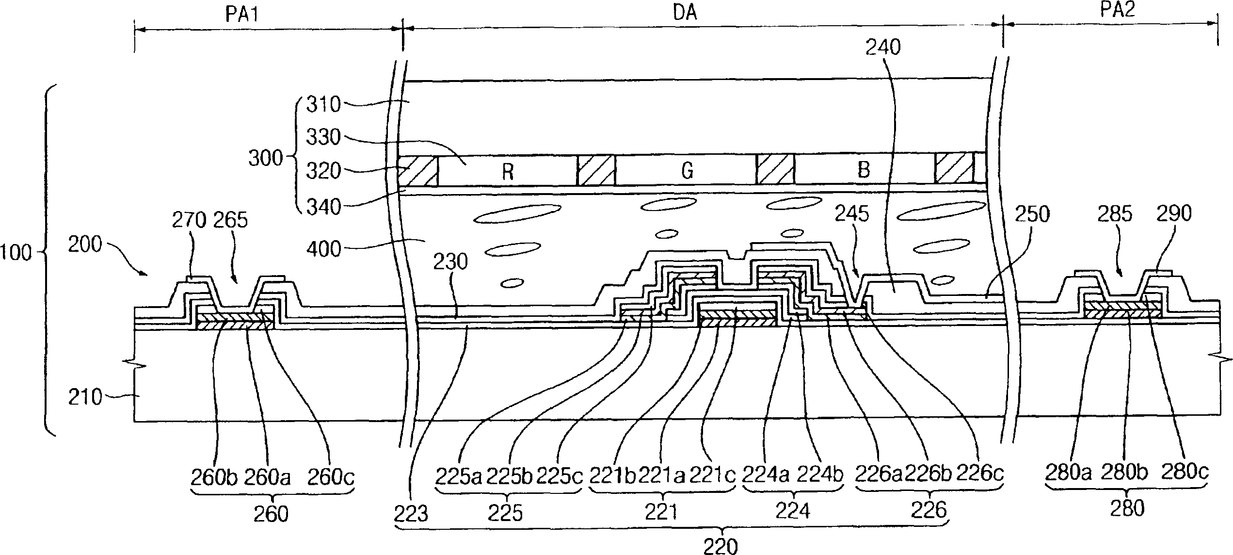
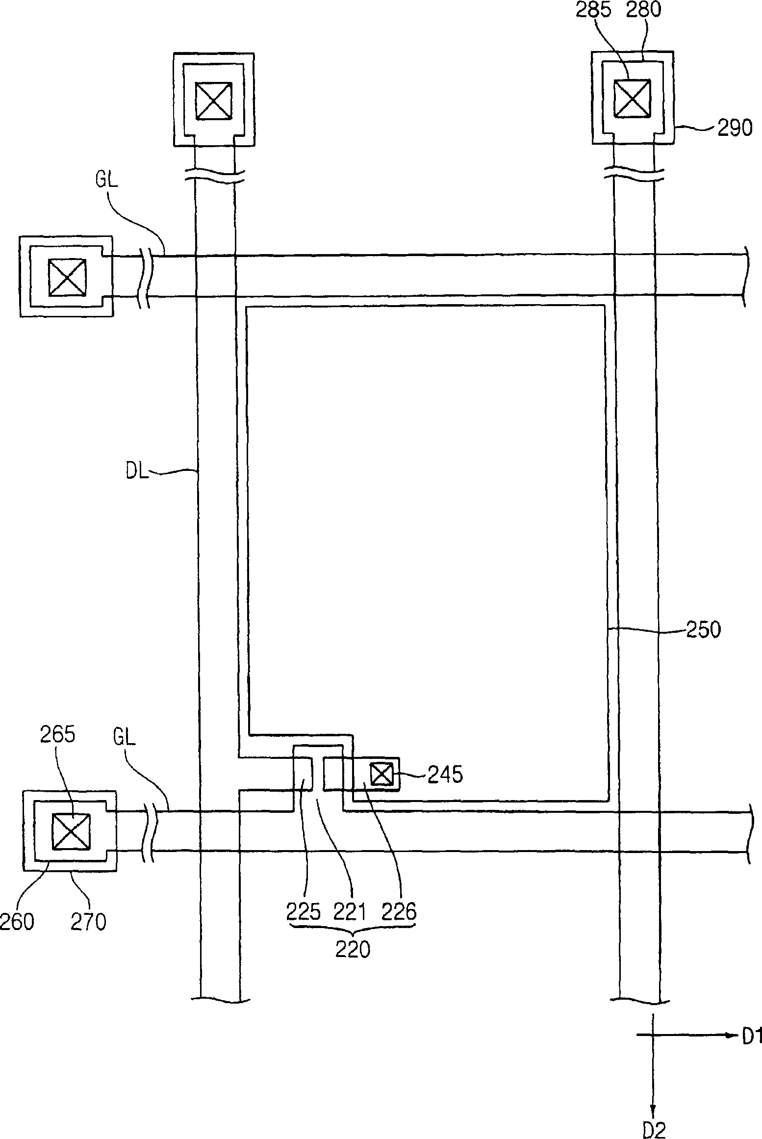
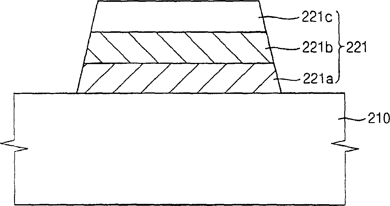
[0036] Figures 4A to 4H Formed for illustration as figure 2 Cross-sectional views of each step of the array substrate shown, Figure 5 Formed for illustration as Figure 4B Cross-sectional view of the reactive sputtering setup for the third metal layer shown, Figure 6 Formed for illustration as Figure 4B A cross-sectional view of the PCVD device for the third metal layer is shown. refer to Figure 4A , the first metal layer 500 is formed on the first insulating substrate 210 . The first metal layer 500 may be formed using aluminum neodymium. In one embodiment of the present invention, the first metal layer 500 is formed by a sputtering process or a chemical vapor deposition (CVD) process using AlNd as a target material. The first metal layer 500 is formed in the entire display area DA, the first peripheral area PA1 and the second peripheral area PA2 on the first insulating substrate 210 .
[0037] refer to Figure 4B , the second metal layer 510 is formed on the f...
Embodiment 2
[0060] Figures 7A to 7G Formed for illustration as figure 1 Cross-sectional views of each step of the array substrate shown, Figure 8 To illustrate etch as Figure 7C A cross-sectional view of the etch bath for the first, second and third metal layers is shown.
[0061] refer to Figure 7A , the first metal layer 500 is formed on the first insulating substrate 210 . The first metal layer 500 may be formed using aluminum neodymium. In one embodiment of the present invention, the first metal layer 500 is formed by a sputtering process using AlNd as a target material and a chemical vapor deposition (CVD) process.
[0062] The second metal layer 510 is formed on the first insulating substrate 210 on which the first metal layer 500 is formed. The second metal layer 510 may be formed using chrome. In one embodiment of the present invention, the second metal layer 510 is formed by a sputtering process using chromium as a target material. The third metal layer 520 is formed ...
PUM
 Abstract
Description
Claims
Application Information