Vertical cavity surface emitting laser and method for fabricating the same

A vertical cavity surface emission and laser technology, applied in lasers, laser parts, semiconductor lasers, etc., can solve problems such as poor laser stability and yield, and achieve easy-to-achieve results

Active Publication Date: 2007-01-24
HIGHER WAY ELECTRONICS +1
View PDF0 Cites 7 Cited by
  • Summary
  • Abstract
  • Description
  • Claims
  • Application Information

AI Technical Summary

Problems solved by technology

However, the stability and yield of VCSELs fabricated by HTO is poor due to the presence of high-temperature steam in the fabrication process, and it is difficult to form a small aperture in the current confinement layer fabricated by HTO

Method used


Image

  • Vertical cavity surface emitting laser and method for fabricating the same
  • Vertical cavity surface emitting laser and method for fabricating the same
  • Vertical cavity surface emitting laser and method for fabricating the same

Examples


Embodiment Construction

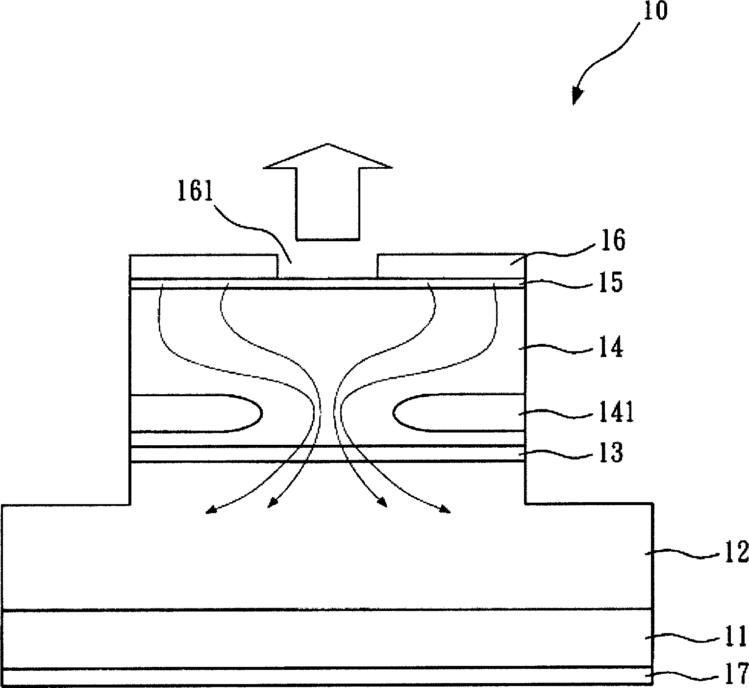
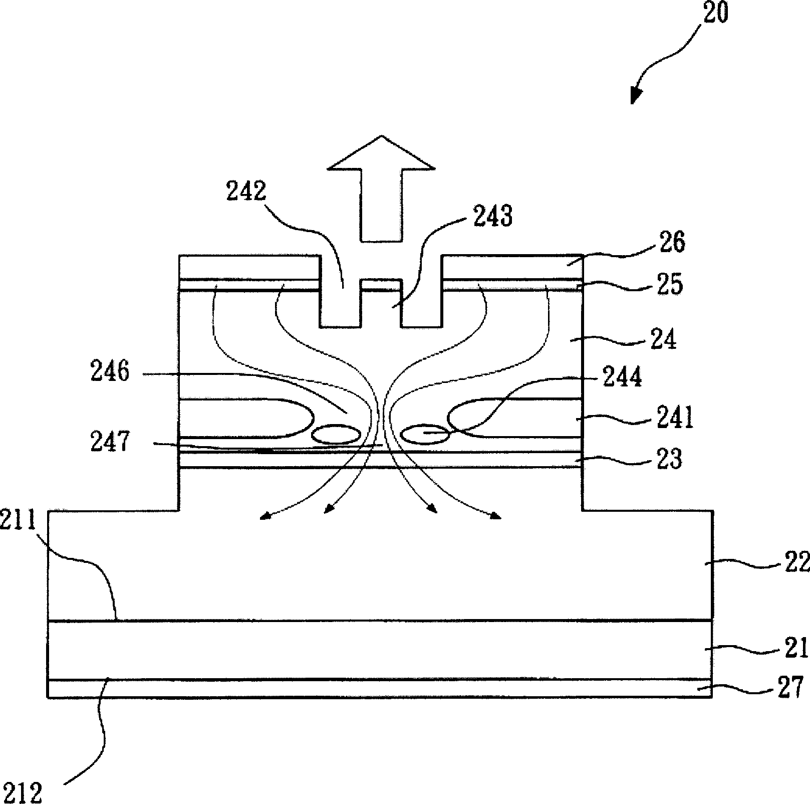
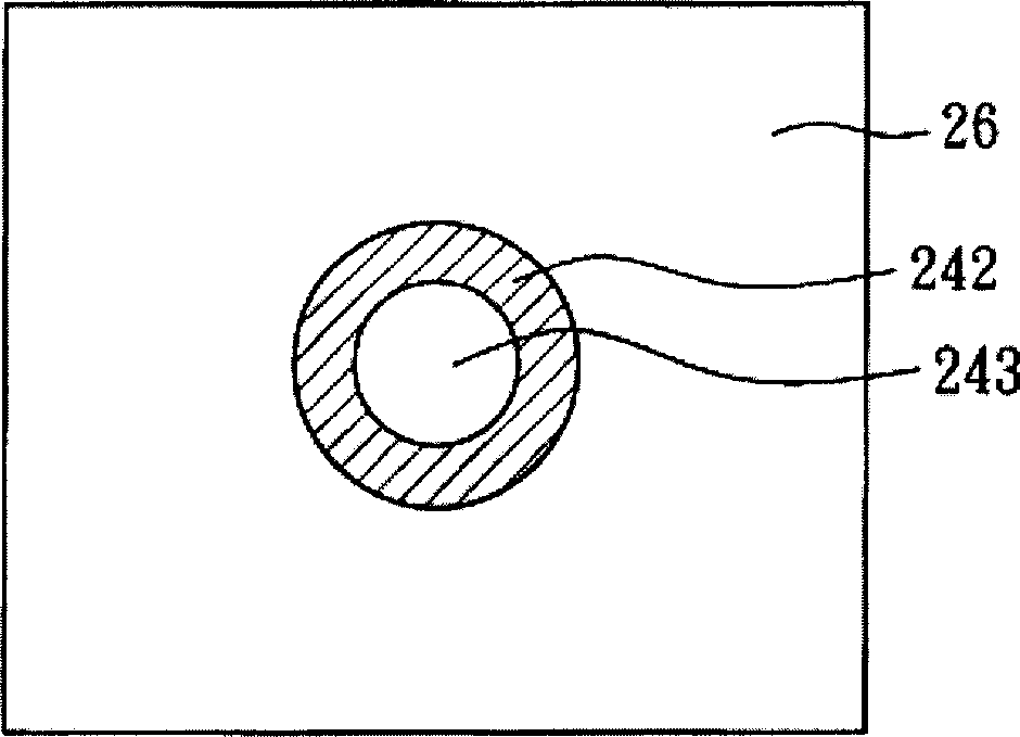
[0012] see figure 2 According to the present invention, the VCSEL 20 includes: a substrate 21, a first reflector 22, an active layer 23, a second reflector 24, a first electrode layer 26 and a second electrode layer 27 . Substrate 21 can be a n + Type GaAs or InP substrate. The substrate 21 has a first surface 211 and a second surface 212 . The first reflector 22 is formed on the first surface 211 of the substrate 21 . The first reflector 22 is a distributed Bragg reflector (DBR) having many pairs of planes. Each pair of layers is formed as graded silicon-doped n + Type Al x Ga (1-x) As / AlAs structure, where x varies from 0.12 to 1, and 1-x varies from 0.88 to 0.

[0013] The active layer 23 is formed on the first reflector 22 . The active layer 23 includes a plurality of undoped GaAs and Al y Quantum wells of GaAs, where y varies from 0.3 to 0.6. The second reflector 24 is formed on the active layer 23 . The second reflector 24 is a distributed Bragg reflector (D...


PUM


Abstract

The invention relates to a vertical cavity surface emitting laser and method for fabricating the same. The vertical cavity surface emitting laser of the invention comprises: a substrate, a first reflector, an active layer, a second reflector, a first electrode layer and a second electrode layer. The second reflector has a first confinement layer with a first aperture and a second confinement layer with a second aperture. The second aperture is smaller than the first aperture. According to the invention, because the second confinement layer is formed by implanting oxygen ion into the second reflector and heating to let the oxygen ion and Al content in the second reflector react to form an oxide layer, the second confinement layer can be used as an optical and electronic confinement layer. Therefore, the width and depth of the second confinement layer can be achieved precisely and easily.

Description

technical field [0001] The present invention relates to a vertical-cavity surface-emitting laser and its manufacturing method, and in particular to a method for manufacturing a vertical-cavity surface-emitting laser with a relatively high yield and a controllable method. Background technique [0002] see figure 1 , the conventional VCSEL 10 includes: a substrate 11, a first reflector 12, an active layer 13, a second reflector 14, a contact layer 15, a first electrode layer 16 and a second electrode Layer 17. The substrate 11 has a first surface and a second surface. The first reflector 12 is formed on the first surface of the substrate 11 . The active layer 13 is formed on the first reflector 12 . The second reflector 14 is formed on the active layer 13 . The contact layer 15 is formed on the second reflector 14 . The first electrode layer 16 is formed on the contact layer 15 . The second electrode layer 17 is formed on the second surface of the substrate 11 . [000...

Claims


Application Information

Patent Timeline
Patent Type & Authority Applications(China)
IPC IPC(8): H01S5/183
CPCH01S5/18391H01S5/2059H01S5/18308H01S5/18311
Inventor 赖利弘赖利温
Owner HIGHER WAY ELECTRONICS
Why Eureka
Try Eureka