Aggregation for manufacturing carbon nanometer tube and thin film, electronic component and method for destroying carbon nanometer tube and carbon nanometer tube selective reaction

A technology for carbon nanotubes and electronic components, which is applied in the fields of manufacturing carbon nanotube aggregates and thin films, electronic components, destroying carbon nanotubes and the selective reaction of carbon nanotubes, and can solve the problem of low device efficiency and burning semiconductor carbon. problems with nanotubes

Inactive Publication Date: 2007-01-31
SONY CORP
View PDF1 Cites 10 Cited by
  • Summary
  • Abstract
  • Description
  • Claims
  • Application Information

AI Technical Summary

Problems solved by technology

The first disadvantage of this method is that the current flowing through the metallic carbon nanotubes generates Joule heating that can burn off adjacent semiconducting carbo

Method used


Image

  • Aggregation for manufacturing carbon nanometer tube and thin film, electronic component and method for destroying carbon nanometer tube and carbon nanometer tube selective reaction
  • Aggregation for manufacturing carbon nanometer tube and thin film, electronic component and method for destroying carbon nanometer tube and carbon nanometer tube selective reaction
  • Aggregation for manufacturing carbon nanometer tube and thin film, electronic component and method for destroying carbon nanometer tube and carbon nanometer tube selective reaction

Examples


example 1

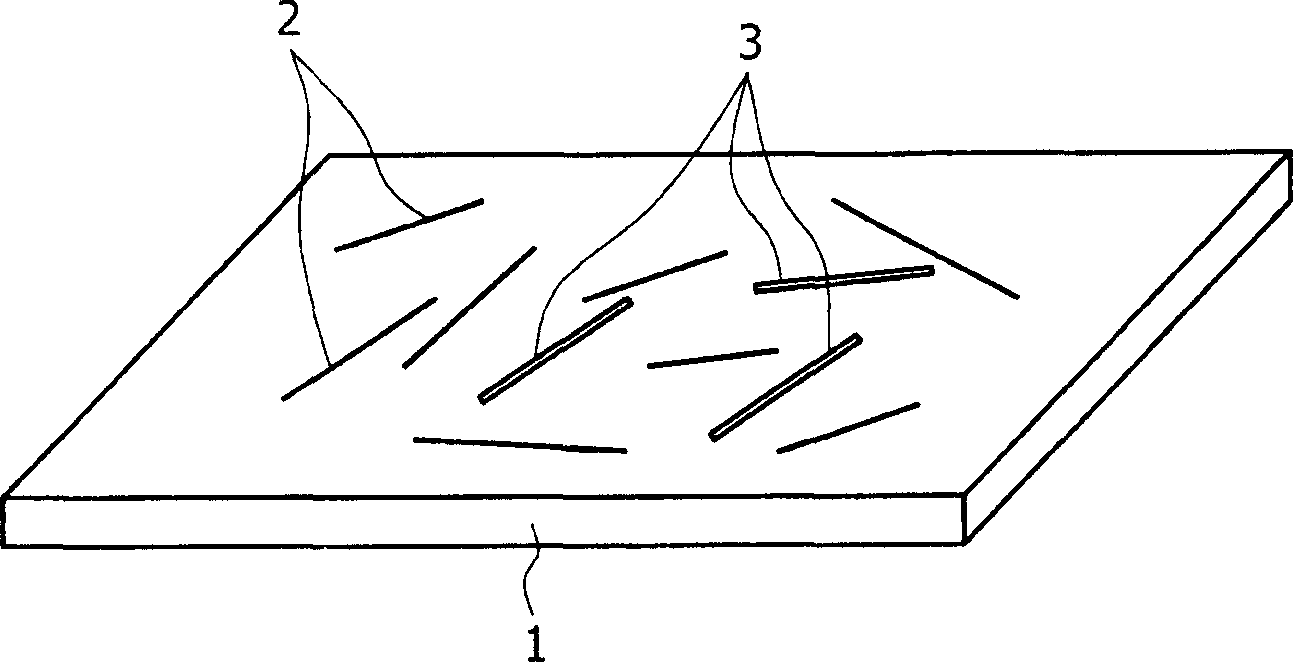
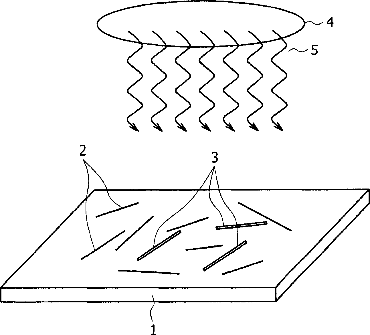
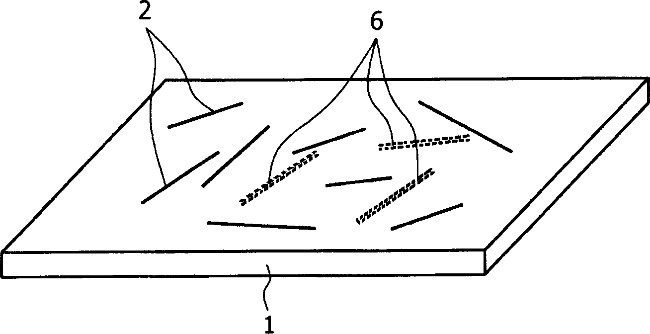
[0122] With a wavelength of 514nm and a power density of 3mW / μm 2 Single-walled carbon nanotubes (commercially available under the trade name SweNT from Southwest Nanotechnologies) were examined by laser irradiation. Figure 10 The obtained Raman spectrum in the RBM (radial breathing mode) region is shown. Due to the third van Hove electronic transition S of semiconducting carbon nanotubes 33 , a laser with the specified energy produces a -1 Raman signal of , and due to the first van Hove electronic transition of metallic carbon nanotubes M 11 , resulting in a 230-300cm -1 Raman signal. For 1590cm -1 The nearby G-mode peaks normalize these Raman spectra. Note that laser irradiation causes the signal from the metallic CNTs to decrease drastically in intensity, while the signal from the semiconducting CNTs remains almost unchanged. Specifically, 80 minutes of irradiation resulted in approximately 85% reduction in intensity of the signal from the metallic carbon nanotubes....

example 2

[0125] In Example 1, note that metallic carbon nanotubes (with smaller diameters) and semiconductive carbon nanotubes (with larger diameters) will bring changes to the Raman spectrum in the RBM region once irradiated with laser light at a wavelength of 514 nm . Some might point out that since carbon nanotubes with smaller diameters are generally more sensitive to laser irradiation, the change in the Raman spectrum is related to the tube size. However, the inventors believe that the illumination effect is determined by the tube type (metallic or semiconductive) rather than the tube size. To prove this point, the inventors irradiated with a laser with a wavelength of 632.8 nm to detect metallic carbon nanotubes (with larger diameter) and semiconductive carbon nanotubes (with smaller diameter) in the RBM region.

[0126] With a wavelength of 632.8nm and a power density of 1mW / μm 2 Laser irradiation inspection of commercial single-walled carbon nanotubes (HiPco). Figure 12 The...


PUM

PropertyMeasurementUnit
Wavelengthaaaaaaaaaa
Diameteraaaaaaaaaa
Diameteraaaaaaaaaa

Abstract

A very easy and thorough method for destroying metallic carbon nanotubes is disclosed here. The method includes: irradiating a mixture of semiconductive carbon nanotubes and metallic carbon nanotubes with an energy beam (such as laser light), thereby selectively destroying the metallic carbon nanotubes or semiconductive carbon nanotubes. Wherein, the energy beam has an energy component resonantly absorbed by metallic carbon nanotubes or semiconducting carbon nanotubes.

Description

technical field [0001] The present invention relates to a method for destroying metallic carbon nanotubes, a method for manufacturing semiconductive carbon nanotube aggregates, a method for manufacturing semiconductive carbon nanotube films, a method for destroying A method for semiconducting carbon nanotubes, a method for producing aggregates of metallic carbon nanotubes, a method for producing thin films of metallic carbon nanotubes, a method for producing electronic devices, and a method for producing carbon nanotubes A method for aggregates, a method for selectively reacting metallic carbon nanotubes, and a method for selectively reacting semiconducting carbon nanotubes. The invention will be applied to thin film transistors (TFTs) in which thin films of carbon nanotubes are used as channel materials. Background technique [0002] Semiconducting single-wall carbon nanotube (semiconducting single-wall carbon nanotube) is one of the promising next-generation semiconductin...

Claims


Application Information

Patent Timeline
IPC IPC(8): C01B31/02B82B3/00
CPCB82Y10/00C01B31/0266B82Y40/00B82Y30/00H01L51/0048Y10S977/742Y10S977/752Y10S977/75C01B32/172H10K85/221
Inventor 黄厚金
Owner SONY CORP
Why Eureka
Try Eureka