Electro-optical device, method of driving electro-optical device, and electronic apparatus

An electro-optical device and driving circuit technology, applied in optics, nonlinear optics, instruments, etc., can solve problems such as picture quality degradation, and achieve the effects of reducing circuit scale, power consumption, and power consumption.

Inactive Publication Date: 2007-01-31
EPSON IMAGING DEVICES CORP
View PDF1 Cites 8 Cited by
  • Summary
  • Abstract
  • Description
  • Claims
  • Application Information

AI Technical Summary

Problems solved by technology

Therefore, there will be a decrease in picture

Method used


Image

  • Electro-optical device, method of driving electro-optical device, and electronic apparatus
  • Electro-optical device, method of driving electro-optical device, and electronic apparatus
  • Electro-optical device, method of driving electro-optical device, and electronic apparatus

Examples


Example

[0054]

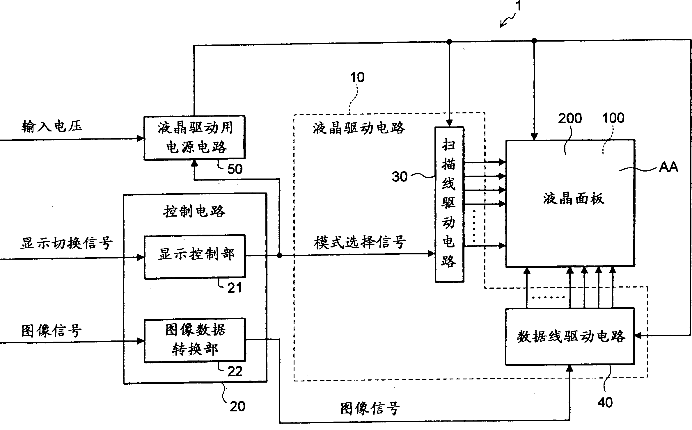
[0055] figure 1 It is a block diagram of the electro-optical device 1 according to the first embodiment of the present invention.

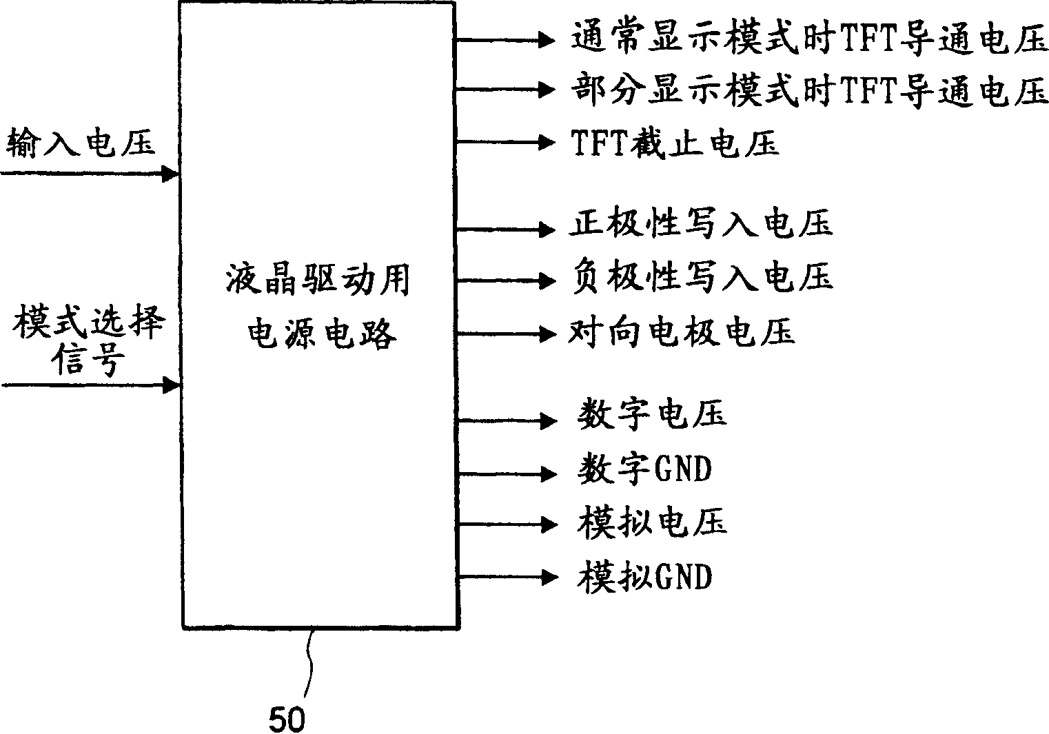
[0056] The electro-optical device 1 has: a liquid crystal panel AA; a liquid crystal driving circuit 10, which is used to drive the liquid crystal panel AA; a control circuit 20, which is used to control the liquid crystal driving circuit 10; and a liquid crystal driving power supply circuit 50, which is used to supply the liquid crystal panel AA and The liquid crystal drive circuit 10 supplies voltage. The liquid crystal drive circuit 10 includes a scan line drive circuit 30 and a data line drive circuit 40 . The control circuit 20 includes a display control unit 21 and an image data conversion unit 22 .

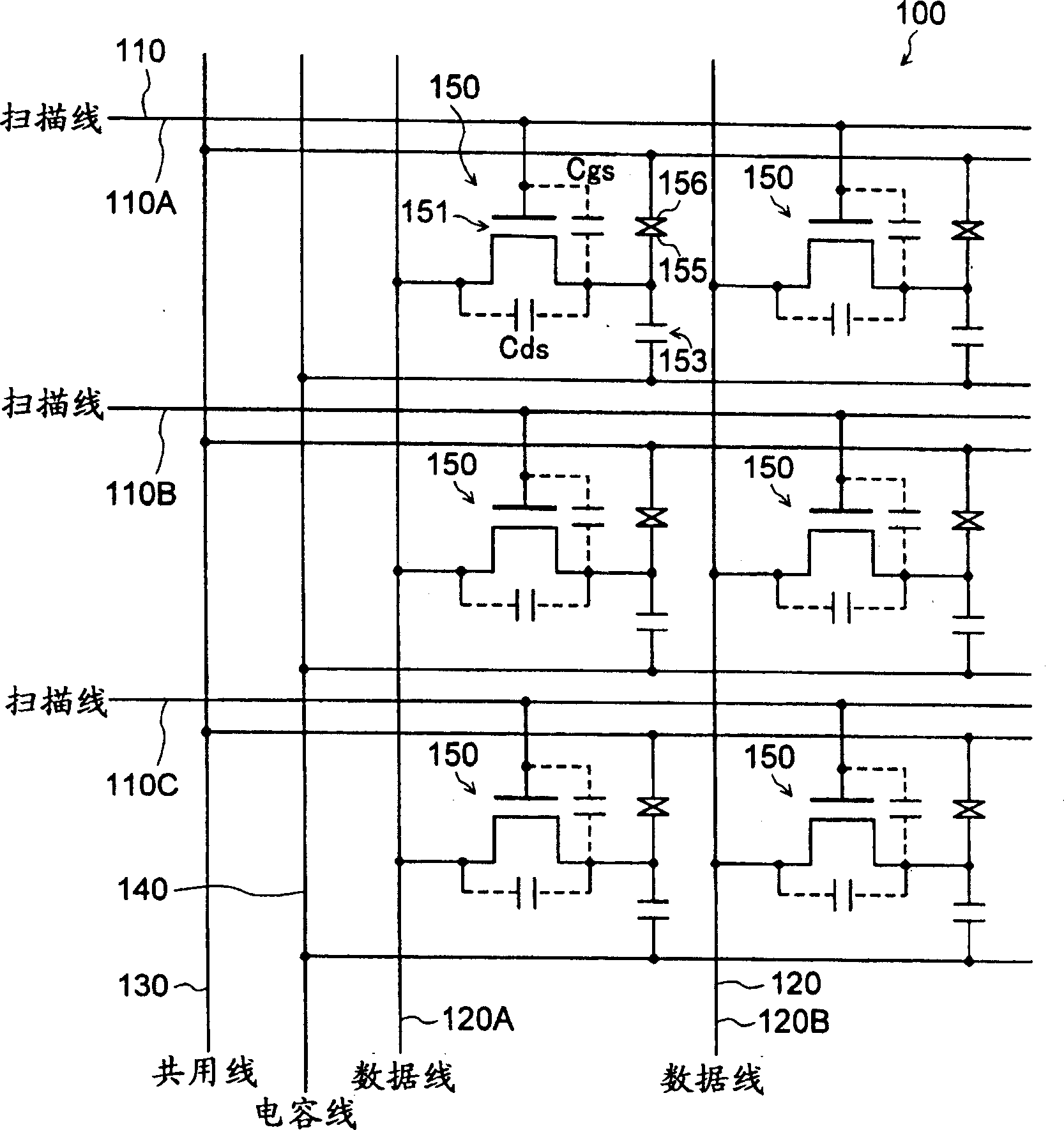
[0057] figure 2 It is a partial enlarged plan view of liquid crystal panel AA.

[0058] LCD panel AA includes (see figure 1 ): an element substrate 100 as a first substrate, in which thin film transistors (hereinafter referred ...

Example

[0110]

[0111] Figure 7 is a circuit diagram of the charge pump circuit 51 according to the second embodiment of the present invention. The charge pump circuit 51 is provided in the power supply circuit 50 for driving liquid crystal, and includes a first charge pump unit circuit 511 and a second charge pump unit circuit 512 .

[0112] The first charge pump unit circuit 511 includes input terminals A and B and an output terminal C. As shown in FIG. The first charge pump unit circuit 511 adds the potential difference between the input terminals A and B to the voltage at the input terminal A, and outputs it from the output terminal C. That is, the first charge pump unit circuit 511 approximately doubles the voltage at the input terminal A, and outputs it from the output terminal C.

[0113] Specifically, the first charge pump unit circuit 511 includes: a capacitor 511A; a switching element 511B for connecting one end of the capacitor 511A to the input terminal A or output t...

Example

[0126]

[0127] Figure 8 is a circuit diagram of the charge pump circuit 52 according to the third embodiment of the present invention. and Figure 7 The difference of the charge pump circuit 51 is the value of the digital voltage that boosts the digital input voltage and outputs it. The charge pump circuit 52 is provided in the liquid crystal drive power supply circuit, and includes a third charge pump unit circuit 521 , a fourth charge pump unit circuit 522 , and a fifth charge pump unit circuit 523 .

[0128] The third charge pump unit circuit 521 has input terminals P and Q and an output terminal R. FIG. The third charge pump unit circuit 521 is used to add the potential difference between the input terminals P and Q to the voltage of the input terminal P, and output it from the output terminal R. That is, the third charge pump unit circuit 521 substantially doubles the voltage at the input terminal, and outputs it from the output terminal R.

[0129] Specifically, ...


PUM


Abstract

An electro-optical device includes a plurality of scanning lines; a plurality of data lines; a plurality of pixels that are provided so as to correspond to intersections between the plurality of scanning lines and the plurality of data lines, each of the pixels has a pixel electrode, and a switching element that allows, when the selection voltage is applied to the scanning line, the data line and the pixel electrode to enter a conductive state; a scanning line driving circuit that supplies a selection voltage for selecting the plurality of scanning lines in a predetermined order; and a data line driving circuit that supplies, when the scanning line is selected, an image signal to the corresponding data line in accordance with a gray-scale level of the corresponding pixel. Further, an entire screen display mode in which an entire screen is displayed and a partial display mode in which a part of an entire screen is set to a display region and the other portion is set to a non-display region are selected, and the scanning line driving circuit supplies a first voltage to the scanning lines of the display region for a predetermined period in the entire screen display mode, and supplies a second voltage to the scanning lines of the display region for a period longer than the predetermined period in the partial display mode.

Description

technical field [0001] The present invention relates to an electro-optical device using an electro-optic substance such as liquid crystal, a driving method of the electro-optic device, and an electronic device having the electro-optic device. Background technique [0002] Conventionally, electro-optical devices such as liquid crystal display devices for displaying images are well known. An electro-optical device includes, for example, a liquid crystal panel and a drive circuit for driving the liquid crystal panel. Such an electro-optical device has, for example, the following configuration. [0003] The electro-optic device includes: a liquid crystal panel; a liquid crystal driving circuit for driving the liquid crystal panel; a control circuit for controlling the liquid crystal driving circuit; and a liquid crystal driving power supply circuit for supplying driving voltage to them. The liquid crystal driving circuit includes a scanning line driving circuit and a data line...

Claims


Application Information

Patent Timeline
IPC IPC(8): G02F1/136G09G3/20
Inventor 清水公司
Owner EPSON IMAGING DEVICES CORP
Why Eureka
Try Eureka