Method for mfg. non-volatile memory body

A manufacturing method, non-volatile technology, applied in semiconductor/solid-state device manufacturing, electrical components, circuits, etc., can solve problems such as component failure, by-product residue, abnormal connection, etc.

Inactive Publication Date: 2007-01-31
MACRONIX INT CO LTD
View PDF0 Cites 0 Cited by
  • Summary
  • Abstract
  • Description
  • Claims
  • Application Information

AI Technical Summary

Problems solved by technology

In this way, when the second polysilicon layer 112 (word line) is subsequently formed, a bridge phenomenon will occur between the word line and the word line, which will cause leakage current (current leakage) and make the device The reliability (reliability) is reduced
[0012] In addition, the problem of residual by-products in the etching process (such as Figure 1B The arrow 114 shown in the figure) will lead to the reaction of the etchant to the etching by-products and the oxide layer 102 in the subsequent process of etching the dielectric layer 110 to form pores penetrating the silicon oxide layer 102 (such as Figure 1D Shown by arrow 116)
Therefore, when forming the second polysilicon layer 112 (word line) subsequently, it will cause the second polysilicon layer 112 (word line) to fill in the void (eg Figure 1E Arrow 118 as shown), so that the second polysilicon layer 112 (word line) is electrically abnormally connected to the substrate 100, thereby causing a short circuit of the element, causing the element to fail, and affecting the product yield

Method used


Image

  • Method for mfg. non-volatile memory body
  • Method for mfg. non-volatile memory body
  • Method for mfg. non-volatile memory body

Examples


Embodiment Construction

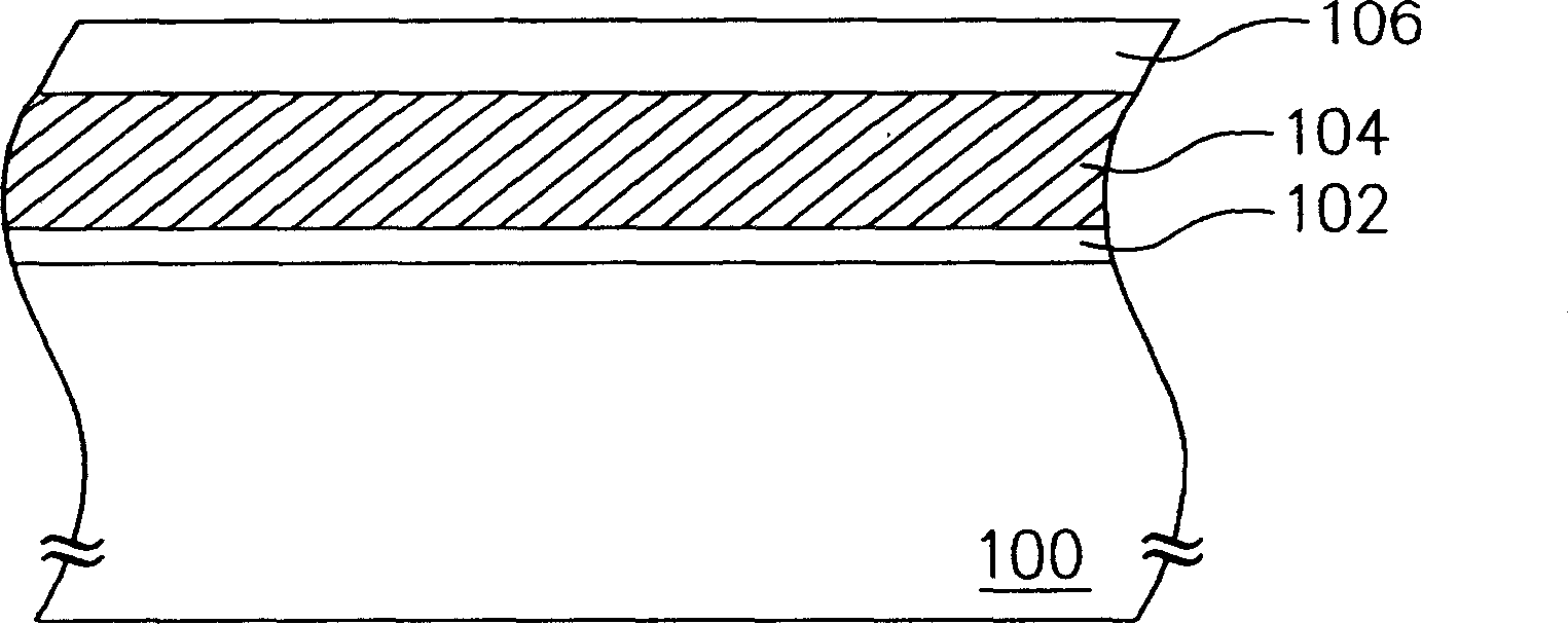
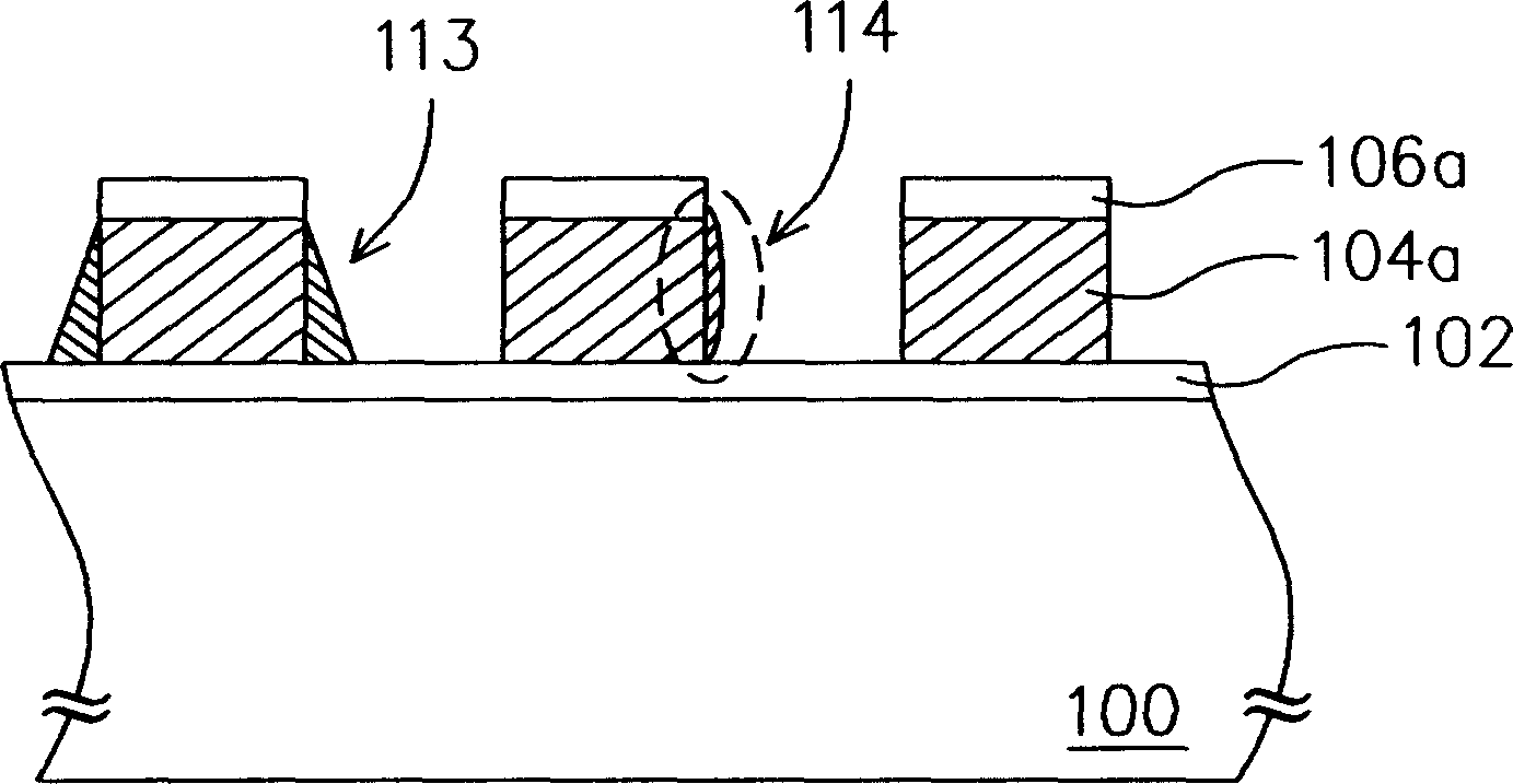
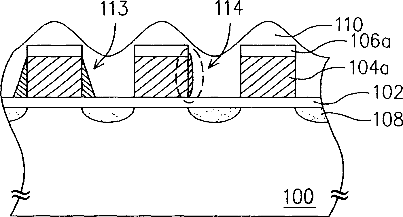
[0039] Figure 2A to Figure 2G It is a schematic cross-sectional view of the manufacturing process of the non-volatile memory according to the present invention.

[0040] First, please refer to Figure 2A , a substrate 200 is provided, and a trench isolation structure (not shown) has been formed in the substrate 200 to define an active region. Next, a dielectric layer 202 is formed on the substrate 200 . Wherein, the dielectric layer 202 can be, for example, a tunnel oxide layer whose material is, for example, silicon oxide, and whose formation method is, for example, thermal oxidation. In one embodiment, the dielectric layer 202 can also be, for example, a composite dielectric layer, such as a silicon oxide / silicon nitride / silicon oxide (oxide-nitride-oxide, ONO) layer, and its formation method An example is chemical vapor deposition.

[0041] After that, please continue to refer to Figure 2A , forming a dummy gate layer 203 on the dielectric layer 202 . Wherein, the m...


PUM


Abstract

The invention relates to a nonvolatile memory manufacturing method, firstly forming a first dielectric layer and a virtual gate layer in turn on a substrate; then, defining plural virtual gates on the virtual gate layer; successively, using the virtual gates as mask to form a doped region in the substrate; forming a second dielectric layer on the first dielectric layer corresponding to the doped region; removing the virtual gate layer to expose part of the first dielectric layer; and forming a conductor layer on the substrate to cover the two dielectric layers.

Description

technical field [0001] The present invention relates to a manufacturing method of a memory, and in particular to a manufacturing method of a non-volatile memory. Background technique [0002] Memory, as the name implies, is a semiconductor device used to store data or data. When the functions of computer microprocessors become stronger and stronger, and the programs and calculations performed by software become larger and larger, the demand for memory becomes higher and higher. In order to manufacture large-capacity and cheap memory to meet this demand The trend of manufacturing memory components and manufacturing processes has become the driving force for semiconductor technology to continue to challenge high integration. [0003] Among various memory products, non-volatile memory, which has the advantage of being able to store, read or erase data multiple times, and that the stored data will not disappear after power failure, has become a A memory component widely used i...

Claims


Application Information

Patent Timeline
IPC IPC(8): H01L21/8247H01L21/336
Inventor 薛铭祥蔡世昌
Owner MACRONIX INT CO LTD
Why Eureka
Try Eureka