Semiconductor device and manufacturing method of the same

A manufacturing method and semiconductor technology, applied in the direction of semiconductor/solid-state device manufacturing, semiconductor devices, semiconductor/solid-state device components, etc., can solve problems such as poor reliability, achieve high yield, improve reliability, and easy processing Effect

Inactive Publication Date: 2007-01-31
SANYO ELECTRIC CO LTD
View PDF1 Cites 3 Cited by
  • Summary
  • Abstract
  • Description
  • Claims
  • Application Information

AI Technical Summary

Problems solved by technology

[0017] In this way, in the conventional structure, damage such as breakage or deformation occurs due to various stresses, impacts, and temperature changes that occur on the semiconductor device, and there is a problem that reliability deteriorates.

Method used


Image

  • Semiconductor device and manufacturing method of the same
  • Semiconductor device and manufacturing method of the same
  • Semiconductor device and manufacturing method of the same

Examples


Embodiment Construction

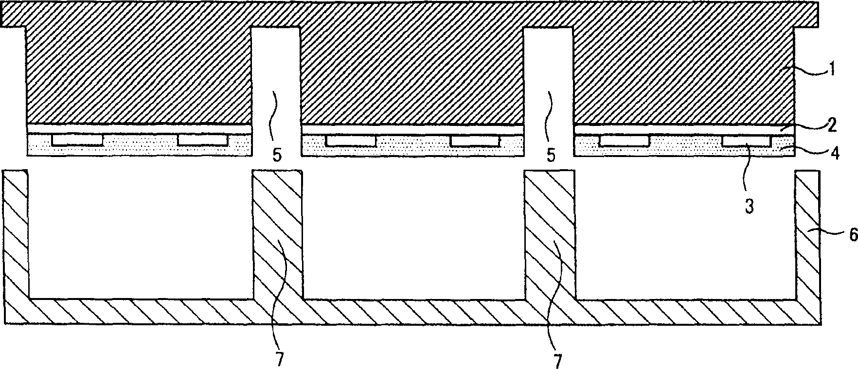
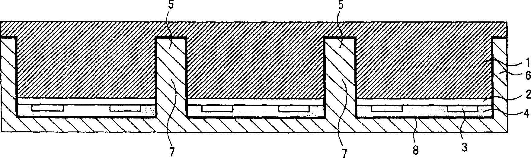
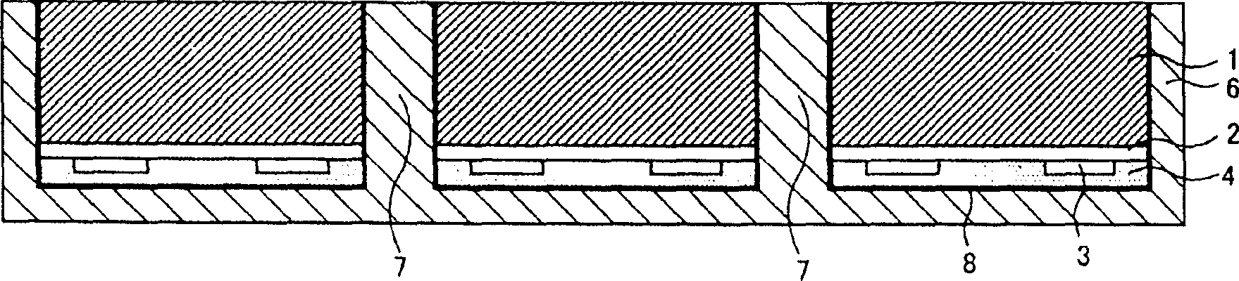
[0039] Embodiments of the present invention will be described in detail below with reference to the drawings. Figure 1 to Figure 8 Each is a cross-sectional view shown in the order of the manufacturing process. in addition, Figure 9It is a plan view of the semiconductor device of the present invention viewed from the back direction, Figure 8 is along Figure 9 The cross-sectional view of the X-X line. In addition, MOS transistors are appropriately formed on the semiconductor substrate, elements such as a plurality of wirings and plugs connecting the wirings, and elements made of a silicon oxide film are separated, but these are not shown in the figure. In addition, since the following processes are performed in the wafer process, a plurality of semiconductor devices 20 are formed at the same time, but for convenience, a process in which three semiconductor devices are formed will be described.

[0040] First, if figure 1 As shown, a first insulating film 2 (eg, a sili...


PUM


Abstract

The invention provides a semiconductor device that provides a high yield and has high reliability. A concave portion (5) is formed on a front surface of a semiconductor substrate (1), and a convex (7) portion is formed on an insulation substrate (6) (such as glass), corresponding to this concave portion (5). Then, the concave portion (5) and the convex portion (7) are engaged to bond the semiconductor substrate (1) and the insulation substrate (6) with an adhesion layer (8) interposed therebetween. A back surface of the semiconductor substrate is back-ground to expose the convex portion (7), and after then, processes such as forming a via hole, forming a penetrating electrode, forming a conductive terminal, and dicing are performed. At this time, the front surface and a sidewall of the semiconductor substrate (1) are covered (protected) with the insulation substrate. The convex portion (7) has a predetermined width and the dicing is performed almost on the center of the convex portion (7).

Description

technical field [0001] The present invention relates to a semiconductor device having excellent processability and high reliability and a method for manufacturing the same. Background technique [0002] In recent years, CSP (Chip Size Package: chip size package) has attracted attention as a three-dimensional packaging technology. A CSP refers to a small package having an outer dimension substantially the same size as that of a semiconductor chip. [0003] Conventionally, a BGA (Ball Grid Array: Ball Grid Array) type semiconductor device is known as a type of CSP. In this BGA-type semiconductor device, a plurality of spherical conductive terminals made of metal members such as solder are arranged in a grid on one main surface of a package, and are electrically connected to a semiconductor chip mounted on the other surface of the package. [0004] And, when this BGA type semiconductor device is incorporated into an electronic device, each conductive terminal is mounted on a ...

Claims


Application Information

Patent Timeline
Patent Type & Authority Applications(China)
IPC IPC(8): H01L23/48H01L23/12H01L21/50
CPCH01L23/3114H01L2924/0105H01L2924/01082H01L2924/09701H01L24/83H01L2924/01029H01L2224/13099H01L2924/01022H01L2924/01013H01L2924/014H01L2224/8385H01L2924/0665H01L2224/2919H01L2924/04941H01L2924/04953H01L24/29H01L2924/01005H01L2924/01033H01L2924/01006H01L21/76898H01L2924/01074H01L2924/01078H01L2224/83894H01L2924/01073H01L2924/07802H01L24/10H01L24/02H01L24/05H01L24/13H01L2224/02372H01L2224/02377H01L2224/05001H01L2224/05008H01L2224/05009H01L2224/05022H01L2224/05124H01L2224/05147H01L2224/05548H01L2224/05624H01L2224/05647H01L2224/0615H01L2224/13H01L2224/13024H01L2224/13025H01L2924/12042H01L2924/13091H01L2924/00H01L2924/3512H01L2924/00014H01L23/12
Inventor 铃木彰三坂荣一
Owner SANYO ELECTRIC CO LTD
Why Eureka
Try Eureka