Check patentability & draft patents in minutes with Patsnap Eureka AI!

Method for forming photoinduced resist pattern

A technology of photoresist and photoresist layer, which is applied in the photoengraving process, optics, optomechanical equipment and other directions of the pattern surface, and can solve the problems of tightening of the end of the straight line, residual pattern of auxiliary, circularization, etc.

Inactive Publication Date: 2007-03-07
UNITED MICROELECTRONICS CORP
View PDF1 Cites 6 Cited by
  • Summary
  • Abstract
  • Description
  • Claims
  • Application Information

AI Technical Summary

Problems solved by technology

[0007] However, the effect of optical proximity correction in the prior art is not good. After exposure, there will still be auxiliary pattern residues placed at right angles to the main pattern, rounded corners, tightened ends of straight lines, and increased or reduced line widths. In other cases, how to use the auxiliary pattern 14 to improve the effect of optical proximity correction is a matter of urgency.

Method used


Image

  • Method for forming photoinduced resist pattern
  • Method for forming photoinduced resist pattern
  • Method for forming photoinduced resist pattern

Examples


Embodiment Construction

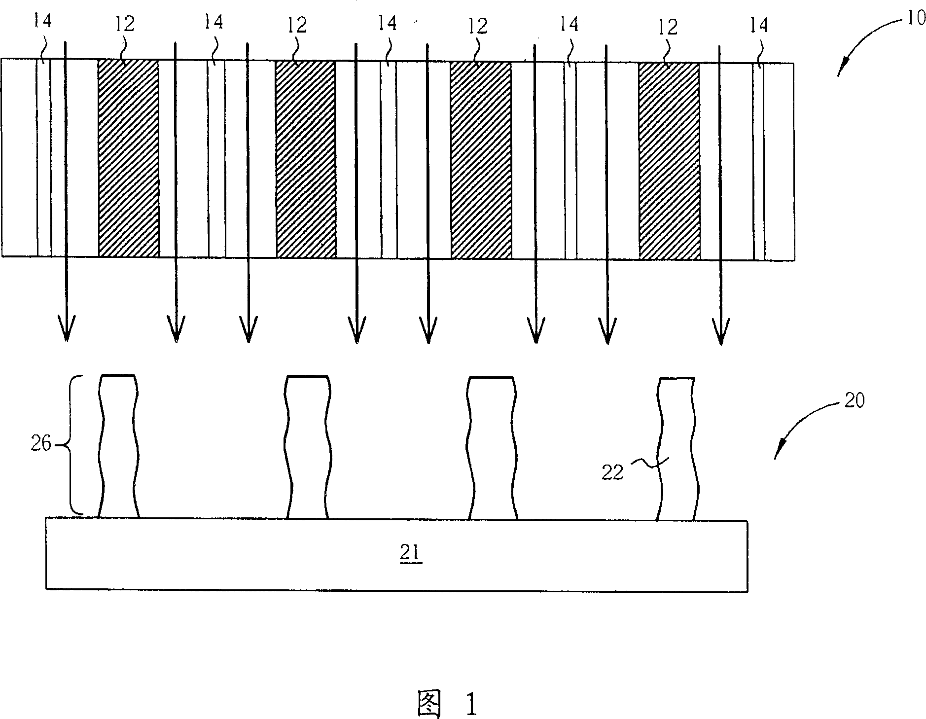
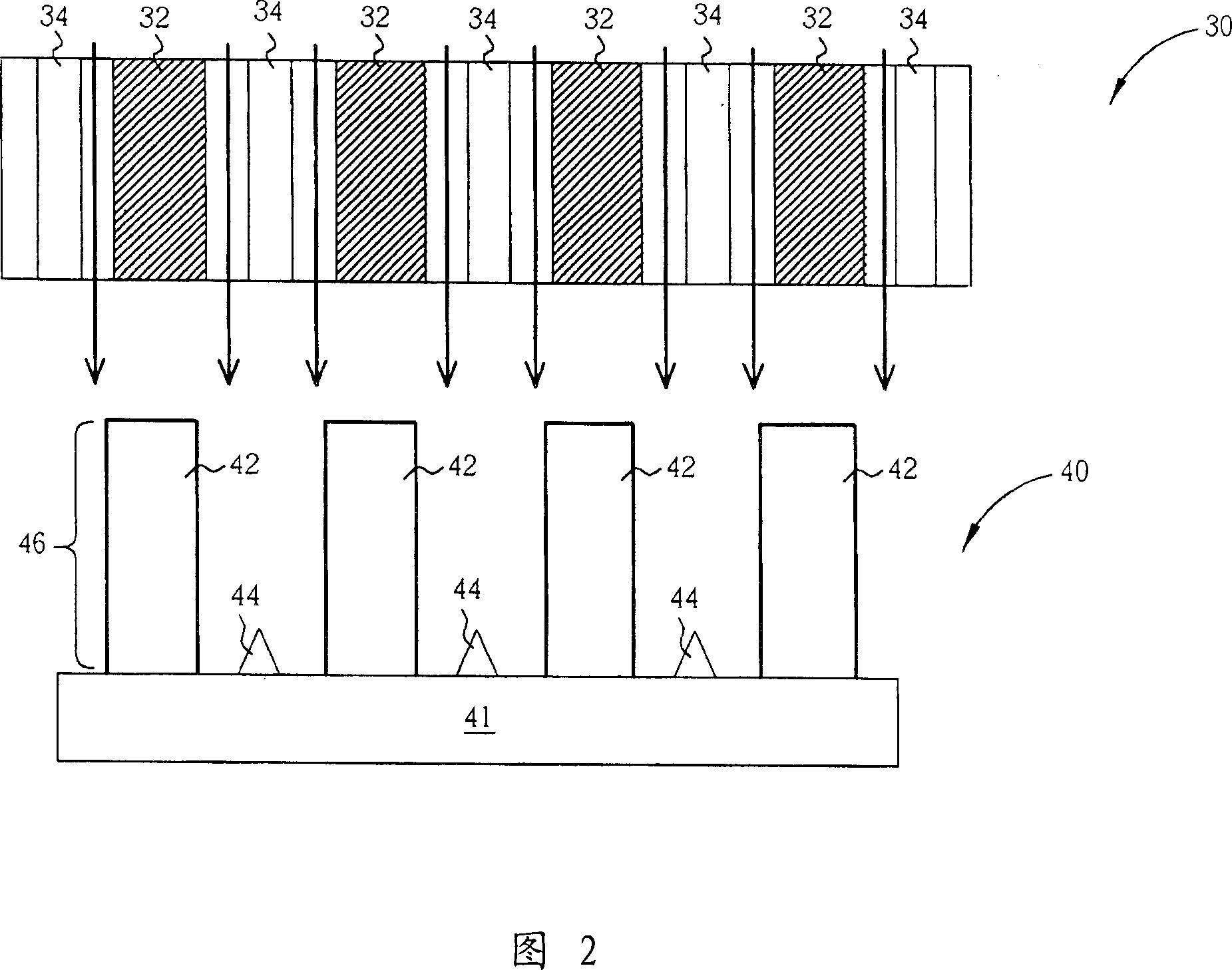
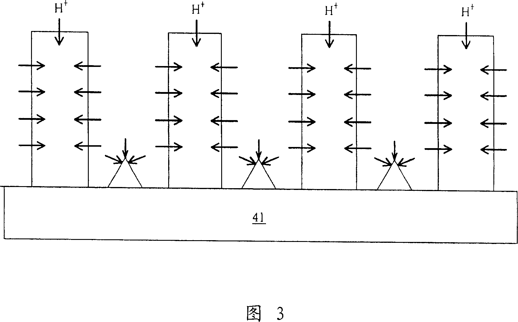
[0021] Please refer to FIGS. 2 to 4. FIGS. 2 to 4 are schematic diagrams of the process of forming a photoresist pattern of the present invention. The photomask 30 in FIG. 2 has at least one main feature 32. There are auxiliary patterns 34 between the main patterns 32. The auxiliary patterns 34 can be composed of serifs, scattering bars, etc. In addition, the semiconductor wafer 40 has a substrate 41. The design of the main pattern 32 must consider the projection magnification of the exposure machine (not shown), the correction of the optical proximity effect (OPE, optical proximity effect), the auxiliary pattern (assistant feature) 34, and the shrinking step ( trim process). After the ideal photomask layout pattern is calculated by the computer, the main pattern 32 is output on the photomask 30. At present, the industry generally uses a projection exposure machine as a photolithography exposure machine, and most of them use CAD computer-aided design to calculate the photomask pat...


PUM


Abstract

This invention provides one method to process photo induced resists on underlay, which comprises the following steps: forming photo induced resists layer on the underlay to provide photo mask with main and assistant patterns for exposure process to make the main and assistant pattern transfer to the photo induced resists layer to form relative photo induced main and assistant patter for contract step; removing the photo induced assistant pattern on the underlay and contracting the main pattern width to make optical effect reduce and art window expend.

Description

Technical field [0001] The present invention relates to a method for forming a photoresist pattern, and more particularly to a method for removing a photoresist auxiliary pattern through a shrinking step of the photoresist pattern. Background technique [0002] In the semiconductor process, in order to smoothly transfer the pattern of integrated circuits to the semiconductor wafer, a series of photomasks must be completed according to the layout data of the circuit pattern in accordance with the design rule of the semiconductor process. Layout pattern design, and then make a photomask pattern on the surface of multiple photomasks according to the layout pattern design of each photomask, and finally apply the photomask to a certain proportion in different processes gradually Transfer to a semiconductor wafer. [0003] Since the critical dimension (CD) of the pattern that can be produced on the photomask is limited by the resolution limit of the optical exposure tool, so when the i...

Claims


Application Information

Patent Timeline
Patent Type & Authority Applications(China)
IPC IPC(8): G03F7/00G03F7/20G03F7/26
Inventor 吴得鸿张圣岳吴承翰
Owner UNITED MICROELECTRONICS CORP
Features
  • R&D
  • Intellectual Property
  • Life Sciences
  • Materials
  • Tech Scout
  • Unparalleled Data Quality
  • Higher Quality Content
  • 60% Fewer Hallucinations
Learn More