Wiring board and ceramic capacitor

A technology for ceramic capacitors and wiring substrates, which can be used in electrical solid devices, circuits, electrical components, etc., and can solve problems such as poor spacing between terminals and difficulty in connecting IC chips.

Active Publication Date: 2007-03-07
NGK SPARK PLUG CO LTD
View PDF2 Cites 8 Cited by
  • Summary
  • Abstract
  • Description
  • Claims
  • Application Information

AI Technical Summary

Problems solved by technology

However, there is a large difference in the pitch between terminals between the terminal group on the IC chip side a

Method used


Image

  • Wiring board and ceramic capacitor
  • Wiring board and ceramic capacitor
  • Wiring board and ceramic capacitor

Examples


no. 1 Embodiment approach

[0112] Hereinafter, a first embodiment in which the wiring board of the present invention is embodied will be described in detail with reference to the drawings.

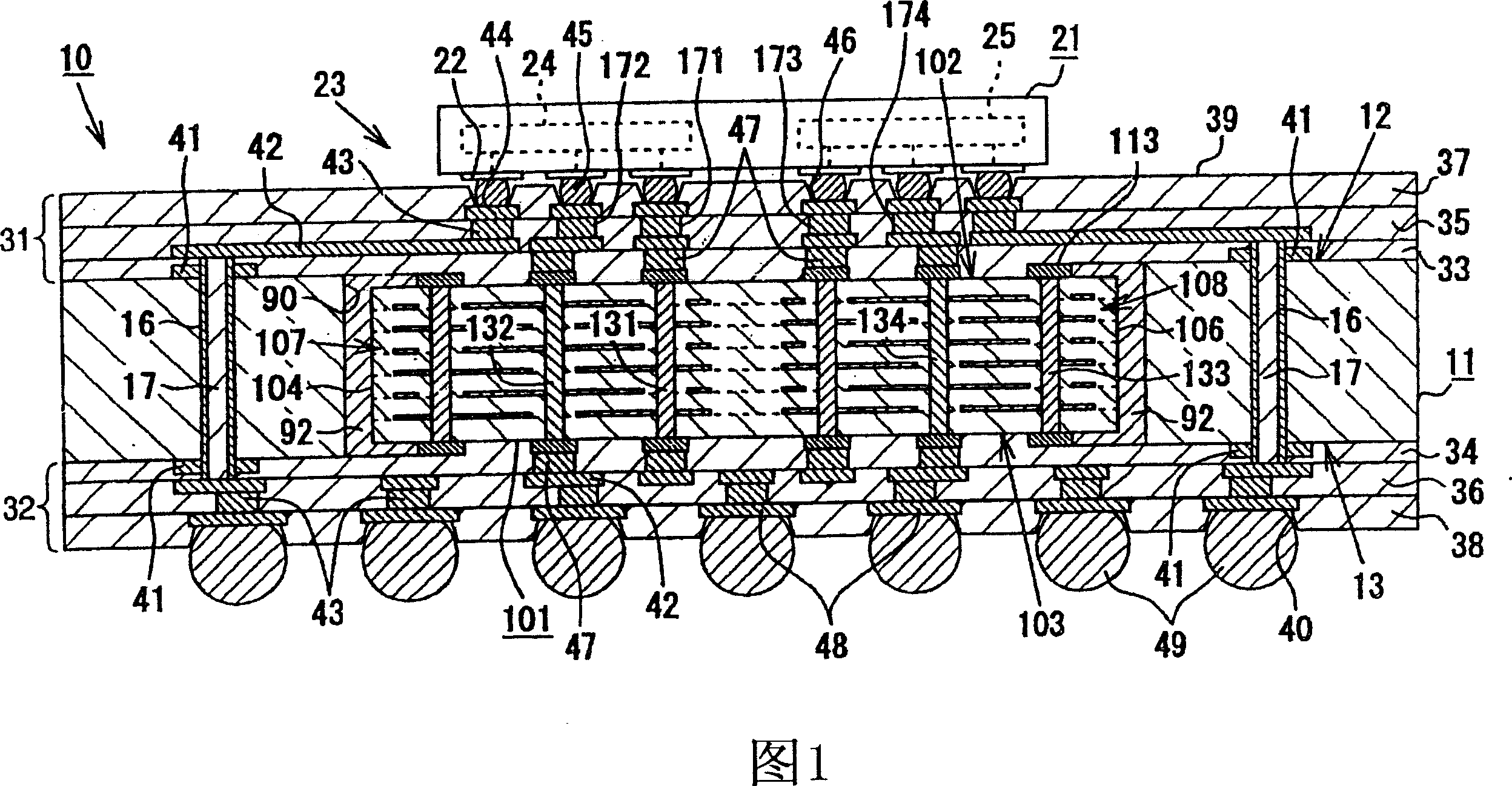
[0113] As shown in FIG. 1 , the wiring substrate 10 of the present embodiment is a wiring substrate for mounting an IC chip, and includes a substantially rectangular plate-shaped substrate core 11 made of epoxy glass, and an upper surface 12 (core) of the substrate core 11. The first construction layer 31 (construction layer) formed on the main surface) and the second construction layer 32 formed on the lower surface 13 of the substrate core 11 (core back surface). Via-hole conductors 16 are formed at a plurality of locations on substrate core 11 . Such via-hole conductors 16 connect and conduct the upper surface 12 side and the lower surface 13 side of the substrate core 11 . In addition, the inside of the via-hole conductor 16 is filled with a sealing body 17 such as epoxy resin, for example. Further, on the upp...

no. 2 Embodiment approach

[0152] Hereinafter, a second embodiment embodying the wiring board of the present invention will be described in detail with reference to the drawings.

[0153] As shown in FIG. 8 , the wiring board 10 ′ of this embodiment has two IC chip mounting regions 51 and 52 (semiconductor integrated circuit element mounting regions) on the surface 9 of the first construction layer 31 . In addition, two IC chips 53 and 54 having only one processor core are respectively mounted on the IC chip mounting regions 51 and 52 instead of the IC chip 21 of the first embodiment described above.

[0154] A part of each first power supply via conductor 131 constituting the capacitor function part 107 is electrically connected to the surface connection terminal 22 of the IC chip 53 through the first power supply electrode terminal 111 and the first power supply conductor part 171 . A part of each first ground via conductor 132 constituting the capacitor function portion 1107 is electrically connected...

no. 3 Embodiment approach

[0179] Hereinafter, a third embodiment in which the wiring board of the present invention is embodied will be described in detail with reference to the drawings.

[0180] The IC chip 21 is different from the wiring board 10 of the first embodiment shown in FIG. 1 in that it has two processor cores 24 and 25 and two I / O circuit units 28 and 29 .

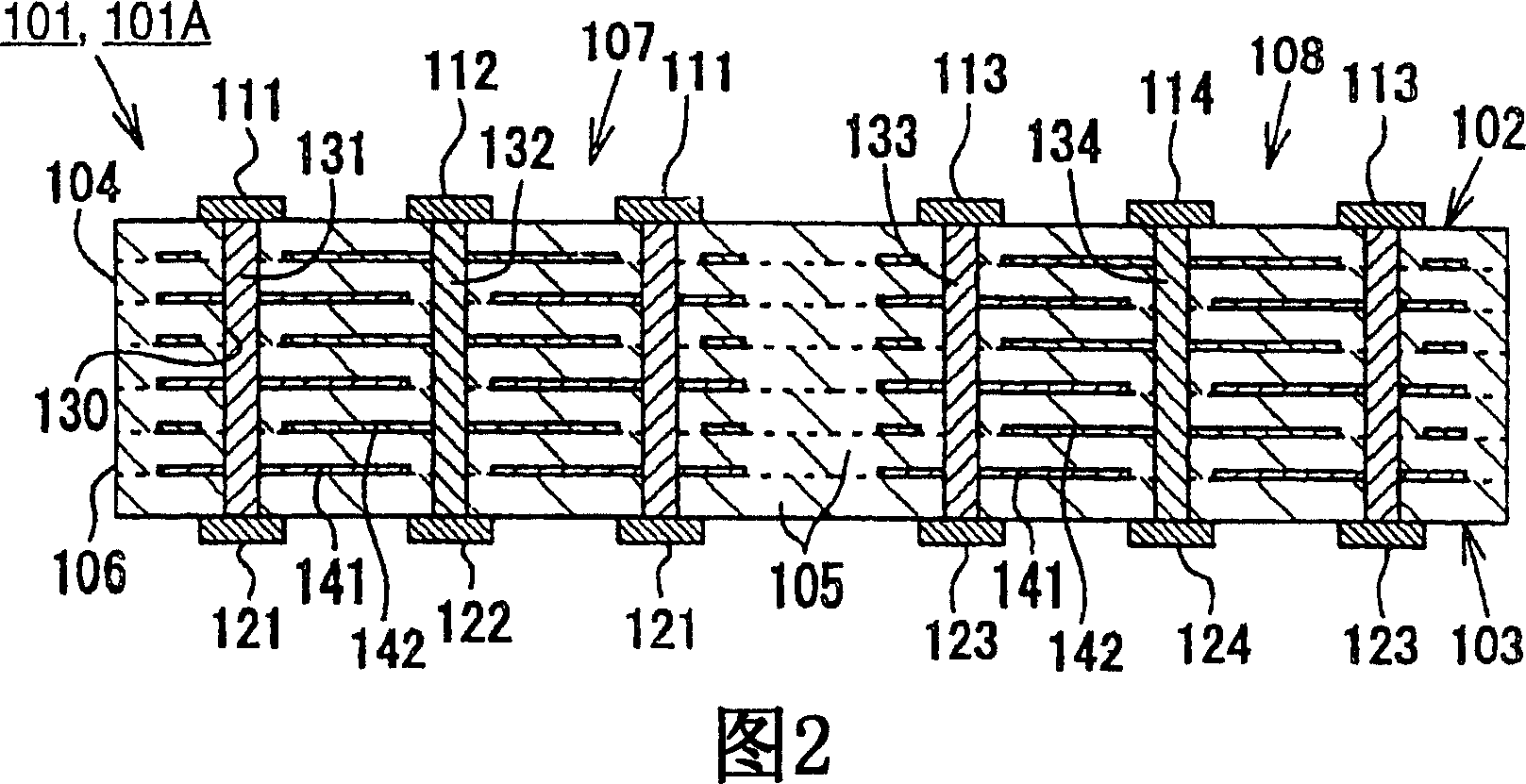
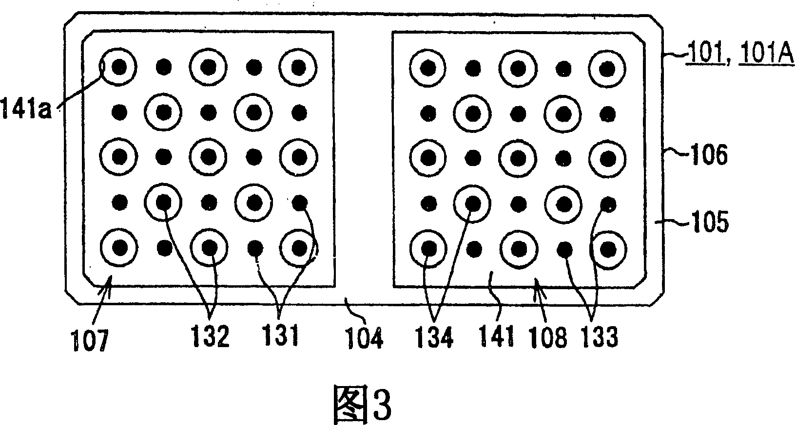
[0181] FIGS. 2 to 4 showing the ceramic capacitor 101 and their descriptions, and FIGS. 5 to 7 and their descriptions showing a manufacturing method are also applicable to the ceramic capacitor 101A of this embodiment. However, the following points are different from those of the first embodiment. The ceramic capacitor 101 is different.

[0182] A ceramic capacitor 101A of this embodiment is shown in FIG. 24 . In the case of the ceramic capacitor 101A of this modified example, a system independent from the processor cores 24, 25 of the IC chip 21 (for supplying power to the I / O circuit sections 28, 29, etc.) is provided on a part the...


PUM

PropertyMeasurementUnit
Thermal expansion coefficientaaaaaaaaaa

Abstract

A wiring board which is easily made multifunctional, minisized, and low-costed. And a capacitor comprising the wiring board is also provided. A wiring board comprising: a board core (11) having a coremain surface (12) and a core reverse surface (13); a capacitor (101) having a capacitor main surface (102) and a capacitor reverse surface (103) and having a structure in which first inner electrodelayers (141) and second inner electrode layers (142) are alternately laminated and arranged via a dielectric layer (105), the capacitor (101) being accommodated in the board core (11) in a state in which the core main surface (12) and the capacitor main surface (102) are oriented on a same side; and a wiring laminated portion (31) having a structure in which interlayer insulating layers (33, 35) andconductor layers (42) are alternately laminated on the core main surface (12) and the capacitor main surface (102), wherein an inductor (251) is formed on or in the capacitor (101).

Description

technical field [0001] The present invention relates to a wiring substrate on which a semiconductor integrated circuit element is mounted, and the use of the wiring substrate, in which a ceramic capacitor is embedded in a substrate core and a build-up layer is formed on the surface of the substrate. of ceramic capacitors. Background technique [0002] In recent years, semiconductor integrated circuit elements (IC chips) used in computer microprocessors and chipsets have become increasingly high-speed and high-functional. Along with this, the number of terminals has increased and the pitch between terminals has tended to become narrower. . Generally, many terminals are densely arranged in an array on the bottom surface of an IC chip, and such a terminal group is flip-chip connected to a terminal group on the motherboard side. However, since there is a large difference in pitch between terminals between the terminal group on the IC chip side and the terminal group on the mot...

Claims


Application Information

Patent Timeline
IPC IPC(8): H05K1/18H05K1/00H01L23/498H01L23/50H01L23/32H01L23/12
CPCH01L2924/14H01L2924/09701H01L2924/15311H01L2224/16H01L2924/01019H01L2224/16235H01L2924/01078H01L2924/3025H01L2924/19042H01L2924/19041
Inventor 小川幸树由利伸治佐藤学杉本康宏
Owner NGK SPARK PLUG CO LTD
Why Eureka
Try Eureka