Electrostatic chuck, thin film manufacturing apparatus having the same, thin film manufacturing method, and substrate surface treatment method

An electrostatic chuck and substrate technology, which can be used in semiconductor/solid-state device manufacturing, circuits, electrical components, etc., and can solve problems such as increased maintenance load.

Inactive Publication Date: 2007-03-21
SEIKO INSTR INC
View PDF1 Cites 5 Cited by
  • Summary
  • Abstract
  • Description
  • Claims
  • Application Information

AI Technical Summary

Problems solved by technology

Therefore, the maintenance load becomes large, and the electrostatic chuck cannot be practically used for catalytic chemical vapor deposition equipment except for a process in a small-scale experimental level

Method used


Image

  • Electrostatic chuck, thin film manufacturing apparatus having the same, thin film manufacturing method, and substrate surface treatment method
  • Electrostatic chuck, thin film manufacturing apparatus having the same, thin film manufacturing method, and substrate surface treatment method
  • Electrostatic chuck, thin film manufacturing apparatus having the same, thin film manufacturing method, and substrate surface treatment method

Examples


Embodiment 1

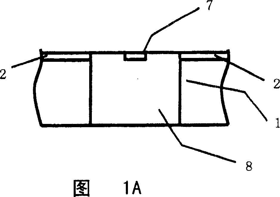
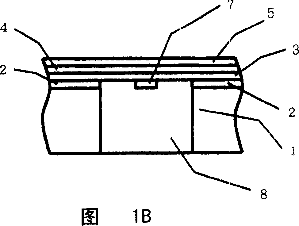
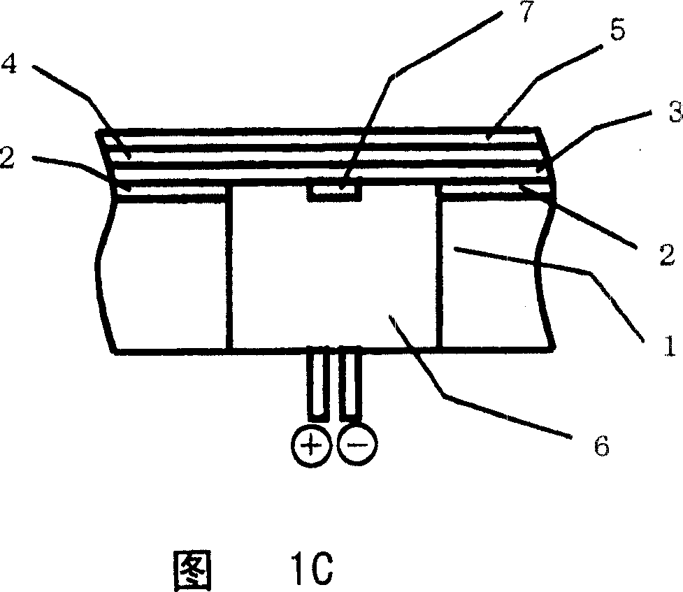
[0023] An electrostatic chuck of an embodiment of the present invention is described using FIGS. 1A to 1C. A first dielectric layer 2 including alumina was thermally sprayed onto an aluminum substrate 1 having a cavity in the central portion, and then an electrode 7 as a conductor was placed in the cavity in the central portion together with a jig 8 ( FIG. 1A ). Then, an internal electrode 3 made of tungsten is thermally sprayed thereon for electrical connection between the electrode 7 and the internal electrode 3 , after which aluminum oxide is thermally sprayed for the second dielectric layer 4 . Although aluminum oxide is used here for the second dielectric layer, magnesium oxide may be used. Further, a silicon nitride film is formed as an insulating film 5 on the second dielectric layer 4 by a chemical vapor deposition process (FIG. 1B). In addition to the silicon nitride film, a film containing silicon nitride or silicon oxide may also be used for the insulating film 5 ....

Embodiment 2

[0029] When using the electrostatic chuck 14 described in example 1 in the catalysis chemical vapor deposition equipment, the electrostatic chuck 14 is set in the catalysis chemical vapor deposition equipment, then by the catalysis chemical vapor deposition equipment can be on the second dielectric A silicon nitride film is deposited on layer 4. In addition, although the adsorption capacity of the electrostatic chuck 14 gradually decreases when the chuck is used for a considerable period of time, when the adsorption capacity decreases, silicon nitride is re-deposited on the surface of the electrostatic chuck 14 by catalytic chemical vapor deposition equipment. membrane, whereby the adsorption capacity can be easily restored. Since the adsorption capacity can be easily restored without removing the electrostatic chuck having reduced adsorption capacity for repolishing, there is an advantage produced by the embodiments of the present invention that an electrostatic chuck with ex...


PUM


Abstract

A difficulty has been given, that is, in a condition that an electrostatic chuck having an oxide layer as a dielectric layer is set in catalytic chemical vapor deposition apparatus, as a silicon thin film is repeatedly deposited on a workpiece held by the electrostatic chuck, adsorbing power of the electrostatic chuck is gradually decreased, and finally the chuck does not adsorb a substrate at all. Thus, a dielectric layer on a surface of the electrostatic chuck is covered with an insulating film containing silicon nitride or silicon oxide. Thus, since damage to a chuck surface can be prevented, the damage being due to hydrogen radicals generated during depositing the silicon film by the catalytic chemical vapor deposition apparatus, even if the silicon film is repeatedly deposited, power for adsorbing the substrate is not decreased, and consequently substrate temperature is stabilized during depositing the silicon film.

Description

technical field [0001] The present invention relates to an electrostatic chuck used in a thin film manufacturing method or a substrate surface treatment method, and more particularly to an electrostatic chuck that can be used for a long period of time without deteriorating the adsorption capacity even when the silicon thin film etc. Under the high temperature environment of hydrogen atoms. Background technique [0002] In the electrostatic chuck of the related art, although a variety of insulators have been proposed for the dielectric layer on the surface of the chuck, especially, in terms of adsorption capacity, controllability at high temperature or thermal expansion coefficient (due to the difference in thermal expansion coefficient between joint surfaces preventability of cracking due to differences) under oxides such as Al 2 o 3 Or MgO is generally used for the dielectric layer (for example, see JP-A-2004-311522 (Patent Document 1)). [0003] Electrostatic chucks in ...

Claims


Application Information

Patent Timeline
Patent Type & Authority Applications(China)
IPC IPC(8): C23C16/00C23C16/448H01L21/68
CPCC23C16/44C23C16/4581C23C16/4586H01L21/6833H01L21/687
Inventor 千本松茂山本修平杉野谷充松村英树增田淳
Owner SEIKO INSTR INC
Why Eureka
Try Eureka