Planar array radiation imaging device

A radiation imaging and area array technology, applied in the field of radiation imaging detection, can solve the problems of difficult large-area detectors, a large number of supporting electronic circuits, complex processes and technologies, etc., to achieve a large effective detection area, improve detection efficiency, shorten the time The effect of scan time

Inactive Publication Date: 2007-03-28
TSINGHUA UNIV
View PDF0 Cites 6 Cited by
  • Summary
  • Abstract
  • Description
  • Claims
  • Application Information

AI Technical Summary

Problems solved by technology

These detectors have complicated process and technology, are not easy to make large-area detectors, have many supporting electronics circuits, and are expensive. These factors restrict their application in large-area area array detector systems.

Method used


Image

  • Planar array radiation imaging device
  • Planar array radiation imaging device

Examples


Embodiment Construction

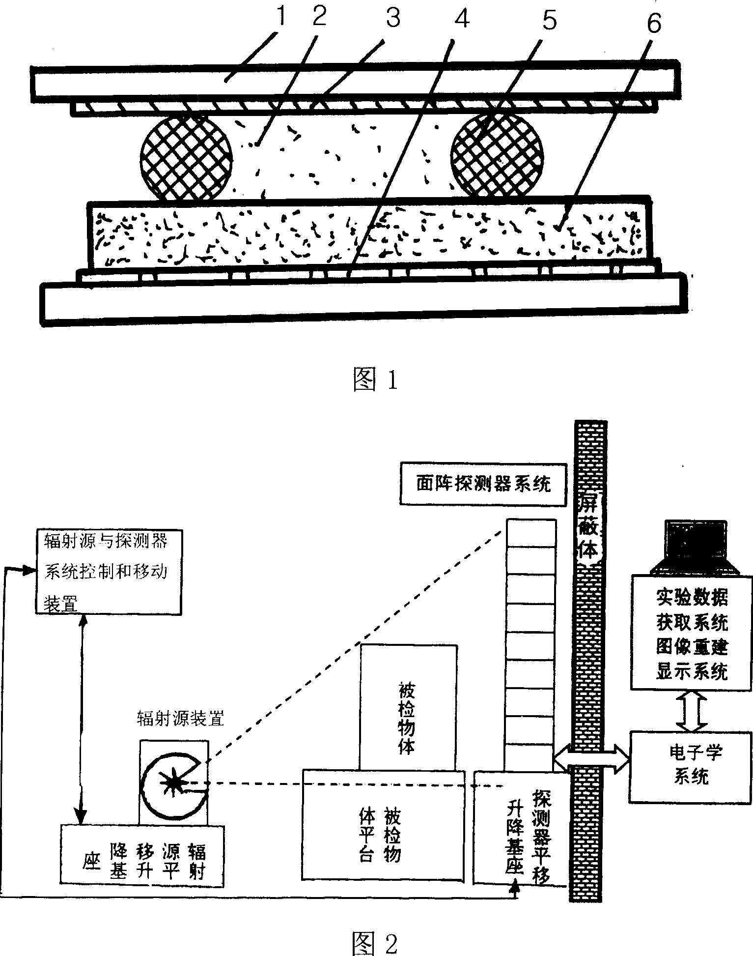
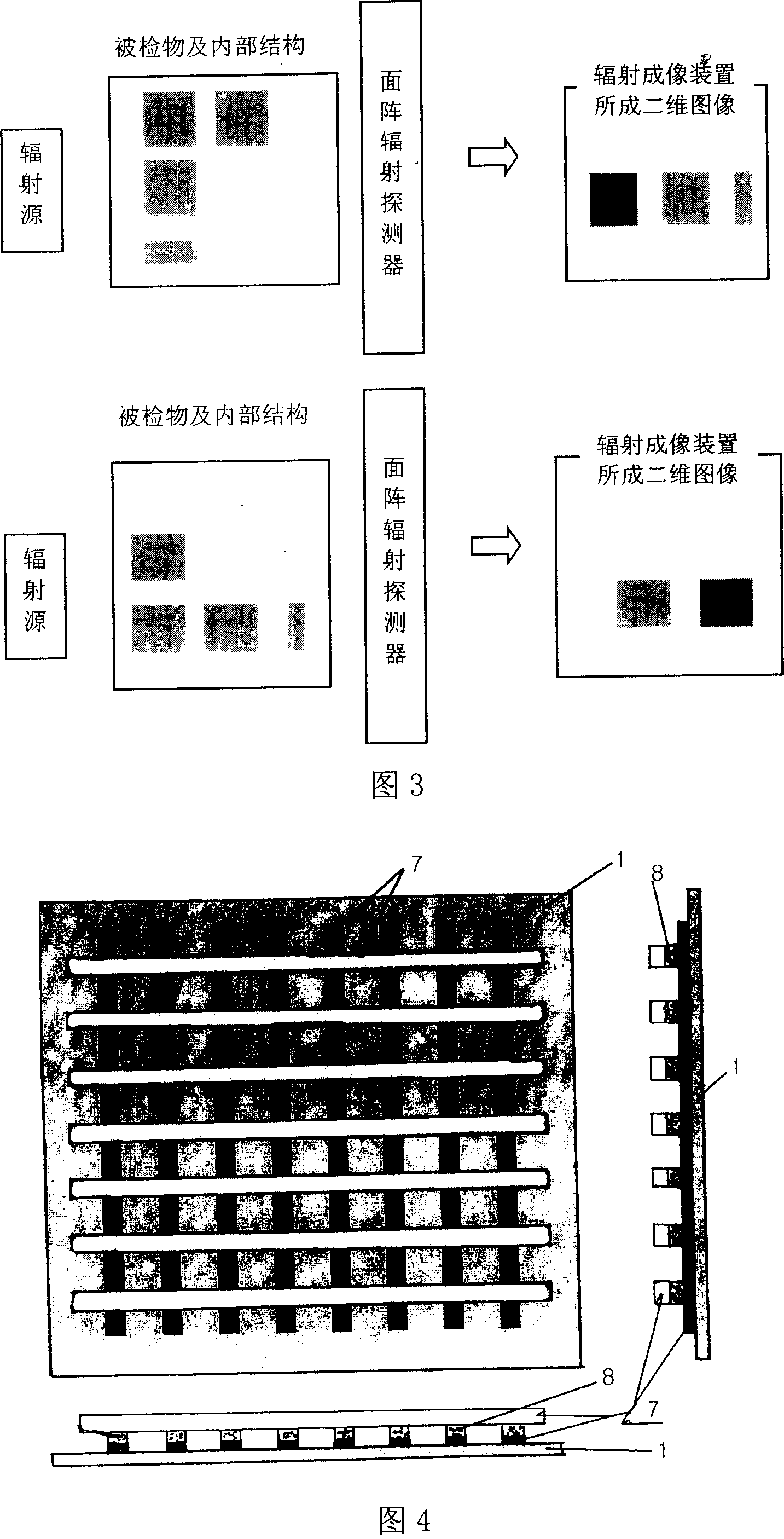
[0024] The present invention proposes an area array radiation imaging device aimed at the deficiencies of the prior art. The test device is a schematic structural diagram of the area array radiation imaging device shown in Figure 2. The object to be detected is placed between a gamma or X-ray radiation source device and The mutual positions of the two-dimensional area array radiation detectors can be adjusted. The test results are shown in the two pictures in Figure 3.

[0025] The main parts of the detector system are described in principle below.

[0026] 1. Two-dimensional radiation detector system for detecting radiation

[0027] A typical structure of the sensitive detection area of ​​a two-dimensional area array radiation detector unit for detecting radiation is shown in Fig. 1 . The sensitive detection unit of the detector is composed of a single layer or multiple layers of equal thickness working gas space separated by insulating wire. There are many choices of worki...


PUM

PropertyMeasurementUnit
Resistivityaaaaaaaaaa
Thicknessaaaaaaaaaa

Abstract

This invention discloses one kind of area array radiation imagery installment which belongs to the radiation imagery survey technology scope, including two-dimensional radiation detector area array, two-dimensional radiation detector necessary electronic installment and empirical data gain system, gamma radiant installment, empirical data processing and picture reconstruction and display system, radiant and detector system relative position control and shifter apparatus. It has big effective survey area, short detecting time, and the detector dead time is short. It may withstand the high-frequency ray radiation, thus greatly reduces the scanning and the imagery time, enhance the system working efficiency. It also has characteristics of low cost, stable performance and convenient maintenance.

Description

technical field [0001] The invention belongs to the technical scope of radiation imaging detection, in particular to an area array radiation imaging device. Background technique [0002] At present, high position resolution area array or linear array detectors commonly used in the field of radiation imaging usually use semiconductors or crystals as sensitive detectors. These detectors have complex process and technology, are not easy to make large-area detectors, have many supporting electronics circuits, and are expensive. These factors restrict their application in large-area area array detector systems. Contents of the invention [0003] The object of the present invention is to propose a kind of area array radiation imaging device aimed at the deficiencies in the prior art, comprising the following parts: [0004] A two-dimensional radiation detector array, a system for detecting radiation; [0005] Two-dimensional radiation detector supporting electronic device and ...

Claims


Application Information

Patent Timeline
IPC IPC(8): G01N23/04G03B42/00
Inventor 岳骞李元景程建平
Owner TSINGHUA UNIV
Why Eureka
Try Eureka