Optical mask pattern correcting method and its formation

A correction method and a technology of photomasks, which are applied in the direction of the original for photomechanical processing, the photoplate process of the pattern surface, optics, etc., can solve the uncontrollable, different, and affect the process yield and reliability component performance, etc. problem, to improve process yield and reliability, and save process cost

Inactive Publication Date: 2007-04-04
POWERCHIP SEMICON CORP
View PDF0 Cites 22 Cited by
  • Summary
  • Abstract
  • Description
  • Claims
  • Application Information

AI Technical Summary

Problems solved by technology

However, when the original patterns to be transferred to the wafer have the same critical dimension but different pattern densities, it is impossible to control the size of the original pattern on the photomask with a single deviation value. After the photolithog

Method used


Image

  • Optical mask pattern correcting method and its formation

Examples


Embodiment Construction

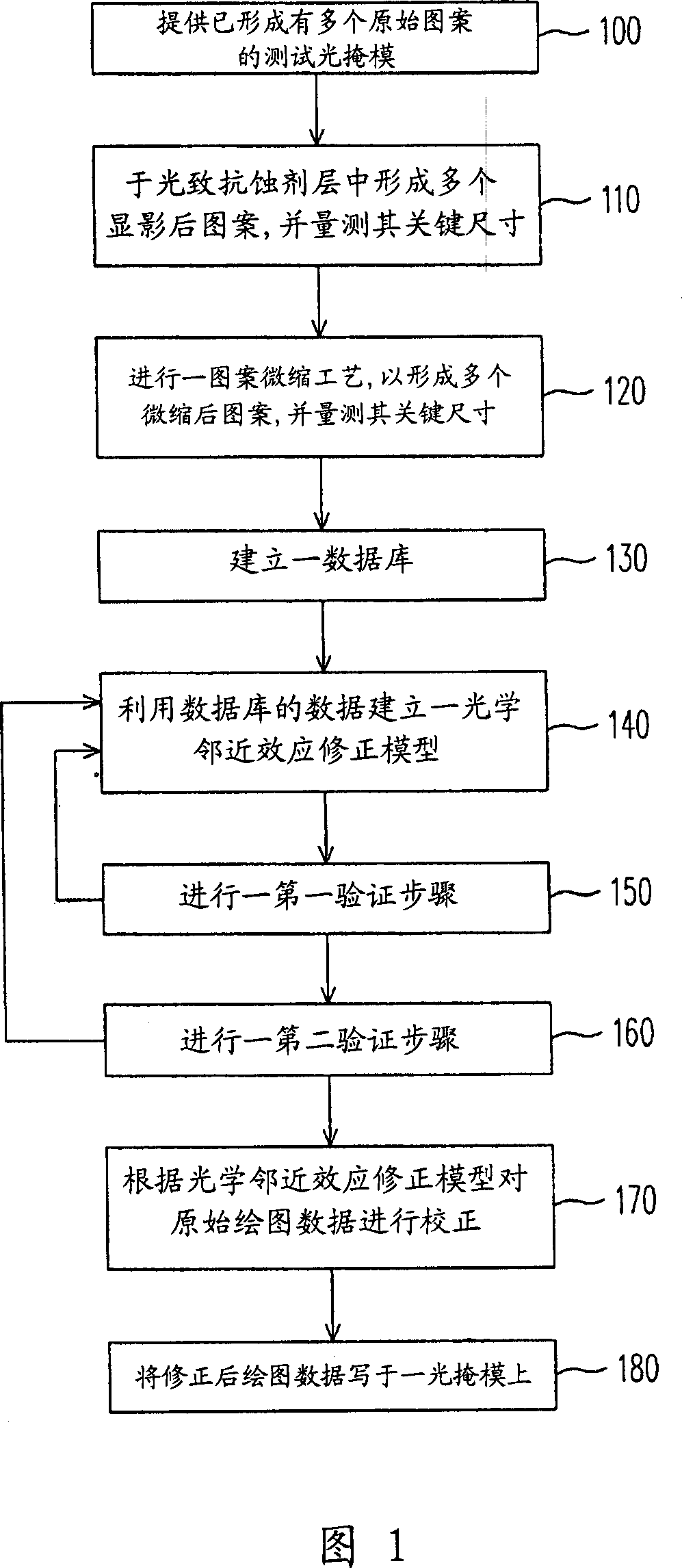
[0021] FIG. 1 is a flowchart of steps of a method for forming a photomask pattern according to an embodiment of the present invention.

[0022] Referring to FIG. 1 , in step 100 , a test photomask is provided, and a plurality of original patterns have been formed on the test photomask according to an original drawing data. For example, the original drawing data of the originally designed circuit layout pattern is written on a test photomask to form a plurality of original patterns on the test photomask. The above-mentioned original drawing data includes key dimensions, pattern density, and line width-to-spacing ratio (Duty Ratio) of the originally designed circuit layout pattern.

[0023] Step 110 , transferring the original pattern on the test photomask to the photoresist layer, so as to form a plurality of developed patterns in the photoresist layer, and measure the critical dimension of each developed pattern. Wherein, the method of transferring the original pattern on the...


PUM


Abstract

A method for calibrating photomask pattern includes providing a test photomask and transferring original pattern on test photomask to the first photoresist layer for obtaining multiple developed pattern then measuring out their first size, carrying out pattern micro process on developed pattern to obtain micro processed pattern then measuring out their second size, calculate out deviate of two said sizes and utilizing two said sizes and deviate as well as original plotting data to form a databank, using databank to set up optical near effect revision model then utilizing said model to calibrate original plotting data for obtaining calibrated plotting data.

Description

technical field [0001] The present invention relates to a method for correcting photolithography and its forming method, in particular to a method for correcting a photomask pattern and its forming method. Background technique [0002] Recently, the semiconductor industry tends to shrink the design and development of circuit components, and one of the most important steps in the entire semiconductor process is photolithography. Anything related to the structure of semiconductor elements, such as the pattern of each layer of thin film, is determined by the photolithography process to determine the size of its Critical Dimension (CD), which is also determined by the development of photolithography process technology. [0003] Nowadays, in response to the development direction of device size reduction and resolution improvement, KrF exposure machine can be used with phase shift mask (Phase Shift Mask, PSM), but in order to better break through the technology node of the process...

Claims


Application Information

Patent Timeline
IPC IPC(8): G03F1/00G03F7/20H01L21/027G06F17/00G03F1/36
Inventor 萧立东
Owner POWERCHIP SEMICON CORP
Why Eureka
Try Eureka