Semiconductor memory

A memory and semiconductor technology, applied in the direction of static memory, read-only memory, digital memory information, etc., can solve the problems of shrinking chips, increasing manufacturing costs, and high unit price of chips, so as to meet high-speed operation, increase operating margin, and shorten memory. The effect of taking time

Inactive Publication Date: 2007-04-04
SHARP KK +1
View PDF1 Cites 0 Cited by
  • Summary
  • Abstract
  • Description
  • Claims
  • Application Information

AI Technical Summary

Problems solved by technology

[0036] However, due to the limitation of setting time, the high-speed transmission path is limited, the operating frequency of the internal clock K cannot be increased, and the timing of output data varies with the clock frequency value, which cannot meet the requirements for high-speed access time.
[0037] In addition, there is no other way to achieve speed-up with the conventional method, or to improve the performance of MOS transistors, or to reduce the size of the chip, etc. to meet the requirements.
[0038] However, in order to improve the performance of MOS transistors, it is necessary to spend a lot of labor, time and money, and it is difficult to meet the requirements of high-speed operation.
[0039] In addition, reducing the size of the chip requires the miniaturization of the process, which leads to an increase in manufacturing costs due to equipment investment, resulting in a high unit price of the chip. Moreover, there is a certain limit to reducing the size using the existing process, so in order to increase the operating speed. Significantly reducing chip size is not realistic

Method used


Image

  • Semiconductor memory
  • Semiconductor memory
  • Semiconductor memory

Examples


Embodiment Construction

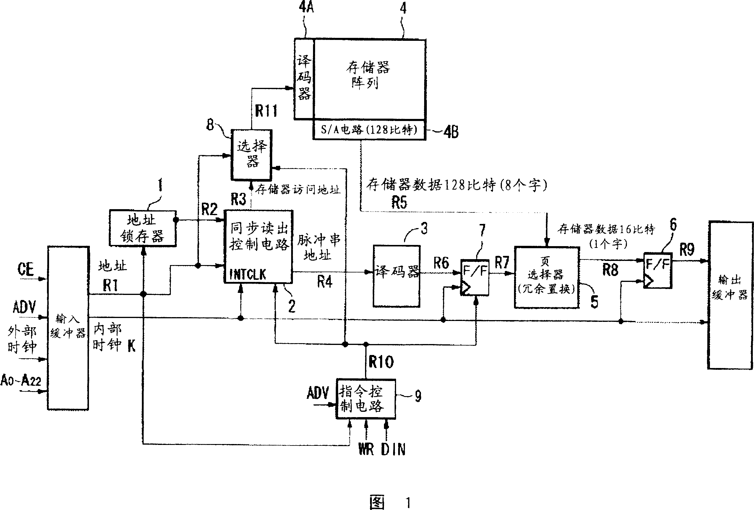
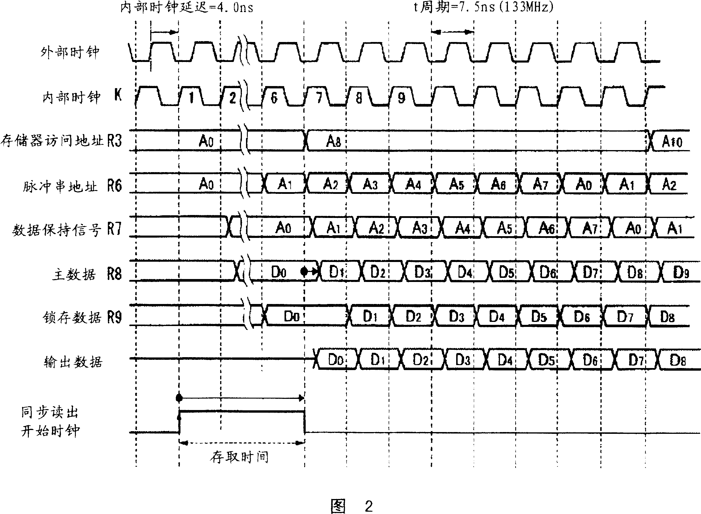
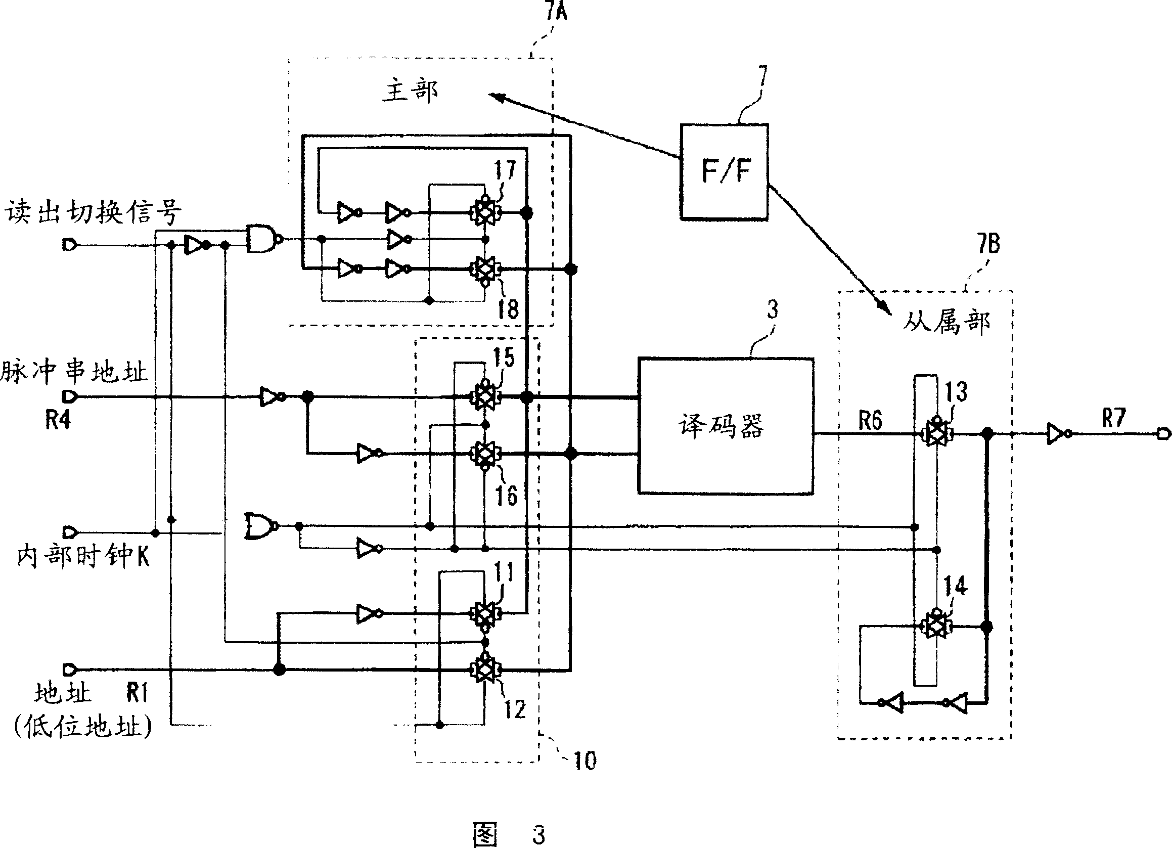
[0064] In the present invention, as shown in FIG. 1, in the synchronous read operation in multiple read modes of the semiconductor memory, a lock for time adjustment is provided at a predetermined position between the synchronous read control circuit 2 and the output latch 6. Register 7, in the past, the increase of the burst address of the synchronous read control circuit 2 is performed from the timing of the predetermined number of clock pulses from the start of synchronous read to the output of data. The internal clock K which is one cycle earlier than the set number of clock pulses starts incrementing the burst address R4.

[0065] That is, in the clock cycle of the internal clock pulse K (minimum number of pulses is the number of internal clock pulses of the above access time plus 1 internal The synchronous readout control circuit 2 changes the burst address R4 at a timing earlier than one internal clock cycle by the number of pulses after the cycle of the clock pulse.

...


PUM


Abstract

A semiconductor memory having a clock-synchronized burst mode read function and including a memory array constituted by a plurality of memory elements; a synchro-read control circuit that outputs, in synchronism with a clock, the upper order address of an address as a memory access address and also outputs, in synchronism with the clock, the lower order address as a burst address; a sense amplifier that outputs the output data of a memory element selected by the memory address; a decoder that decodes the burst address; an address latch that latches the burst address in synchronism with the clock; a page selector that holds the output data and selects the held output data in accordance with the burst address of the address latch; and an output latch that latches the output data in synchronism with the clock.

Description

technical field [0001] The present invention relates to a semiconductor storage device that stores data in correspondence with addresses, and more particularly to a semiconductor memory that has a function of reading data in a burst mode. Background technique [0002] Among semiconductor memories, flash memory is an electrically erasable memory with non-volatile characteristics such that the stored data is not lost when the power is cut off. Since it does not require a battery to keep data, it is mostly used in small portable devices in recent years. (especially mobile phone) storage device. [0003] Currently, the third generation of mobile phones is in service, applications such as Java (registered trademark) application execution and animation processing are diversified, and demands for larger internal memory, higher speed, and lower power consumption are increasing. [0004] In the flash memory described above, there is a synchronous burst read mode (hereinafter referre...

Claims


Application Information

Patent Timeline
IPC IPC(8): G11C11/401G11C11/407G11C16/02G11C16/06G11C7/10
CPCG11C7/1072G11C7/1027G11C16/32G11C16/34G11C16/06G11C16/08G11C16/26
Inventor 前田贤吾谷川明西山增治大堀庄一平野诚高岛洋的场伸次浅野正通
Owner SHARP KK
Why Eureka
Try Eureka