A method to fabricate high resistance value polysilicon resistance in high voltage IC

A high-voltage integrated circuit, polysilicon resistor technology, applied in the manufacture of circuits, electrical components, semiconductor/solid-state devices, etc., can solve the problems of increasing production costs, affecting efficiency, wasting time, etc., to achieve stable resistance, reduce costs, and in-plane Good uniformity

Active Publication Date: 2007-05-16
SHANGHAI HUAHONG GRACE SEMICON MFG CORP
View PDF0 Cites 4 Cited by
  • Summary
  • Abstract
  • Description
  • Claims
  • Application Information

AI Technical Summary

Problems solved by technology

In this way, the final resistance value can be obtained, but because this layer of special injection mask is required, a series of process steps such as coating, development, injection, and glue removal will be added, which not only increases the production cost but also wastes time. affect efficiency

Method used


Image

  • A method to fabricate high resistance value polysilicon resistance in high voltage IC
  • A method to fabricate high resistance value polysilicon resistance in high voltage IC

Examples


Embodiment Construction

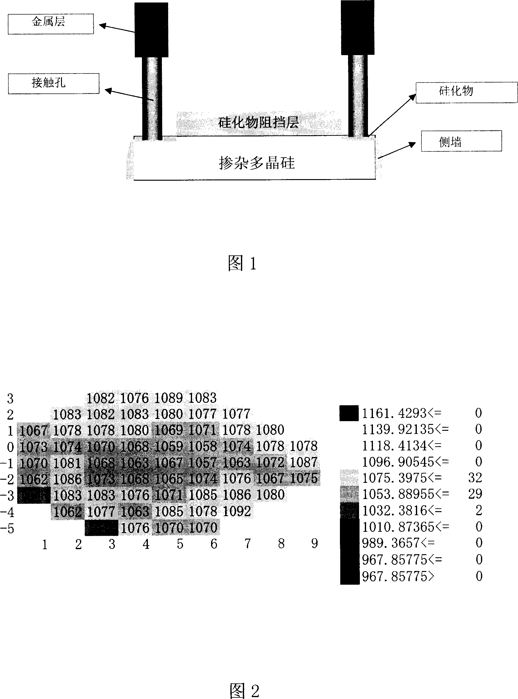
[0017] The main technical points of the method for manufacturing high-resistance polysilicon resistors in high-voltage integrated circuits of the present invention are: the deposition process of in-situ arsenic-doped polysilicon, the doping concentration and deposition process parameters affect the resistance value of the resistor itself; The subsequent thermal process mainly affects the distribution of impurities in polysilicon.

[0018] The doped polysilicon (DOPOS) is deposited by low pressure plasma enhanced chemical vapor deposition (LPCVD).

[0019] The specific process parameters are as follows: S i h 4 (Silane) flow rate 1600cm 3 / min, pH 3 (phosphine) flow rate 12.8cm 3 / min, time 34.5 minutes, furnace temperature 530°C, pressure 0.0997Kpa.

[0020] The follow-up thermal process after the DOPOS deposition affects the distribution of impurities in the polysilicon as mentioned above, and then affects the resistance value. In the present invention, the subsequent hi...


PUM


Abstract

The disclosed manufacture method for high-resistance multicrystal sensistor in high-voltage IC comprises: using the non-silicatized in-situ doped-arsenic multicrystal grid material as the resistance element; etching the high-resistance area and the grid; finally, taking the thermal process after material sedimentation. This invention can obtain 1000omega block resistance element.

Description

technical field [0001] The invention relates to a manufacturing process method of a semiconductor integrated circuit, in particular to a method for manufacturing a high-resistance polysilicon resistor in a high-voltage integrated circuit. Background technique [0002] High-value resistor elements are often used in high-voltage integrated circuit products, and are directly integrated inside the integrated circuit to reduce the geometric size of the chip. Doped or undoped polysilicon is usually used as the high resistance element material, which is called high resistance polysilicon (HR Poly). In order to obtain the target resistance value, a special implantation mask is generally required, and photoresist is used to block other areas, and ion implantation is performed on the resistance area to adjust its resistance value. In this way, the final resistance value can be obtained, but because this layer of special injection mask is required, a series of process steps such as co...

Claims


Application Information

Patent Timeline
Patent Type & Authority Applications(China)
IPC IPC(8): H01L21/82
Inventor 俞波王飞郑萍
Owner SHANGHAI HUAHONG GRACE SEMICON MFG CORP
Why Eureka
Try Eureka