Component mounting method and component mounting apparatus

An installation method and a technology for installation devices, which are applied in the direction of assembling printed circuits, electrical components, electrical components, etc. with electrical components, can solve problems such as no compensation control, increased electrical positives, poor conduction, etc., and achieve the effect of shortening the installation time

Inactive Publication Date: 2007-05-16
PANASONIC CORP
View PDF1 Cites 24 Cited by
  • Summary
  • Abstract
  • Description
  • Claims
  • Application Information

AI Technical Summary

Problems solved by technology

[0008] However, IC chips tend to be thinner, and in the processing stage from wafer dicing to IC chip processing, processing strain tends to remain in the IC chip, which tends to impair the planarity of the IC chip.
In addition, if a thinner IC chip is sucked and held by a suction nozzle, since the negative pressure of suction and holding is concentrated on the central part of the IC chip, it is easy to lift the central part upwards and cause warping.
[0009] Even if it is intended to mount such a thinned IC chip, which tends to be corrugated due to processing strain or warped due to adsorption and holding, on a substrate by using the mounting method related to the above-mentioned prior art, there is a problem that the The state in which the formed protruding electrodes contact the multiple substrate electrodes formed on the substrate also differs depending on the location, and the protruding electrodes and the substrate electrodes cannot be bonded with high precision.
However, there is a problem that the heating by the heater is also transferred to the side of the platform holding the substrate through the suction nozzle and the IC chip, and thermal expansion on the side of the platform is not considered.
Also, since thermal expansion on the platform side occurs later than on the mounting head side, no control is in place to compensate for it
[0011] Similarly, if the heating is stopped and the cooling is performed, there is a problem that, although the shrinkage occurs on the side of the mounting head, in order to compensate for it, the control of lowering the mounting head is performed, but the mounting platform is not considered. side contraction
[0012] In addition, if the descending operation to compensate for shrinkage during cooling causes expansion on the mounting head side due to heat transfer from the platform side that occurs late in cooling, there is a problem that the molten portion that is solidifying will be damaged. The force acting in the peeling direction creates an interface or an opening formed by a crack in the joint portion, resulting in poor joints such as increased electric current and poor conduction.

Method used


Image

  • Component mounting method and component mounting apparatus
  • Component mounting method and component mounting apparatus
  • Component mounting method and component mounting apparatus

Examples


Embodiment Construction

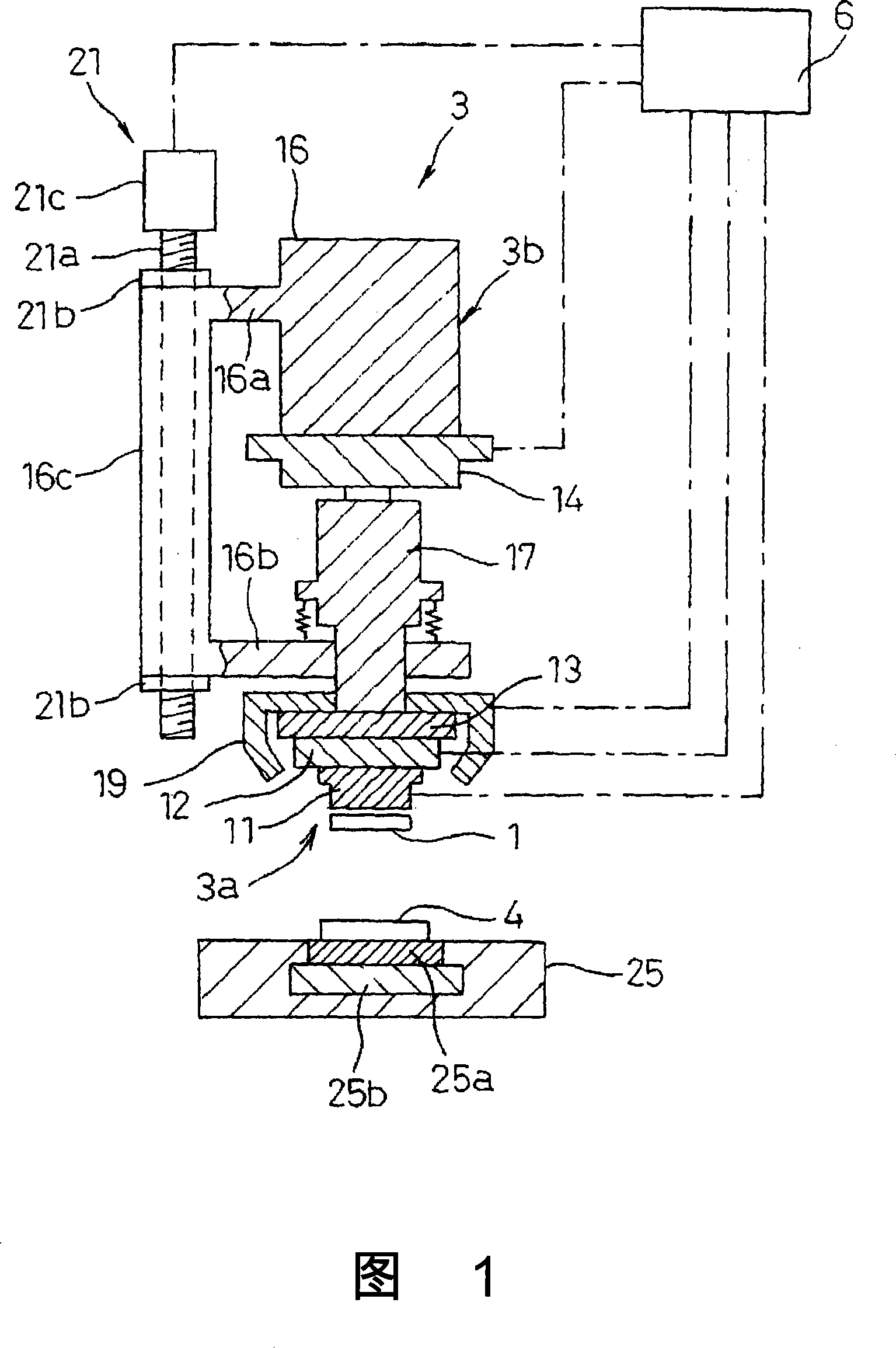
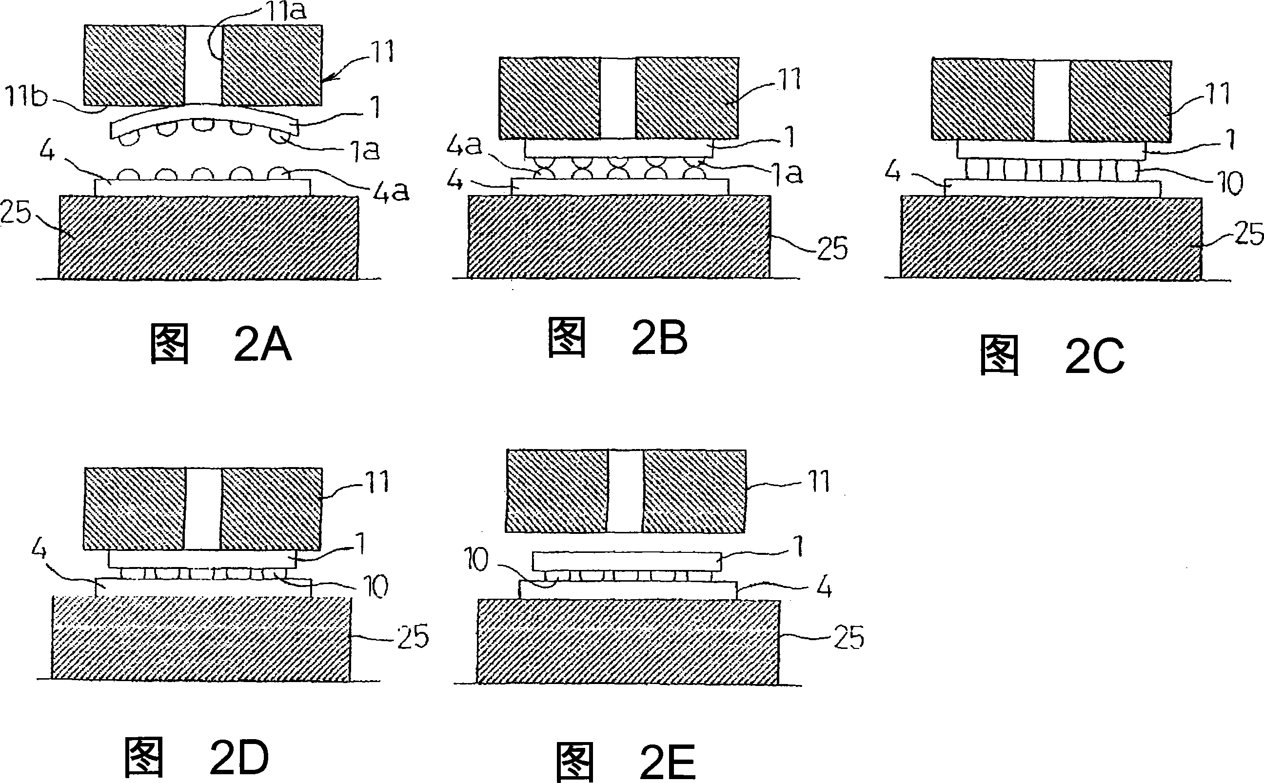
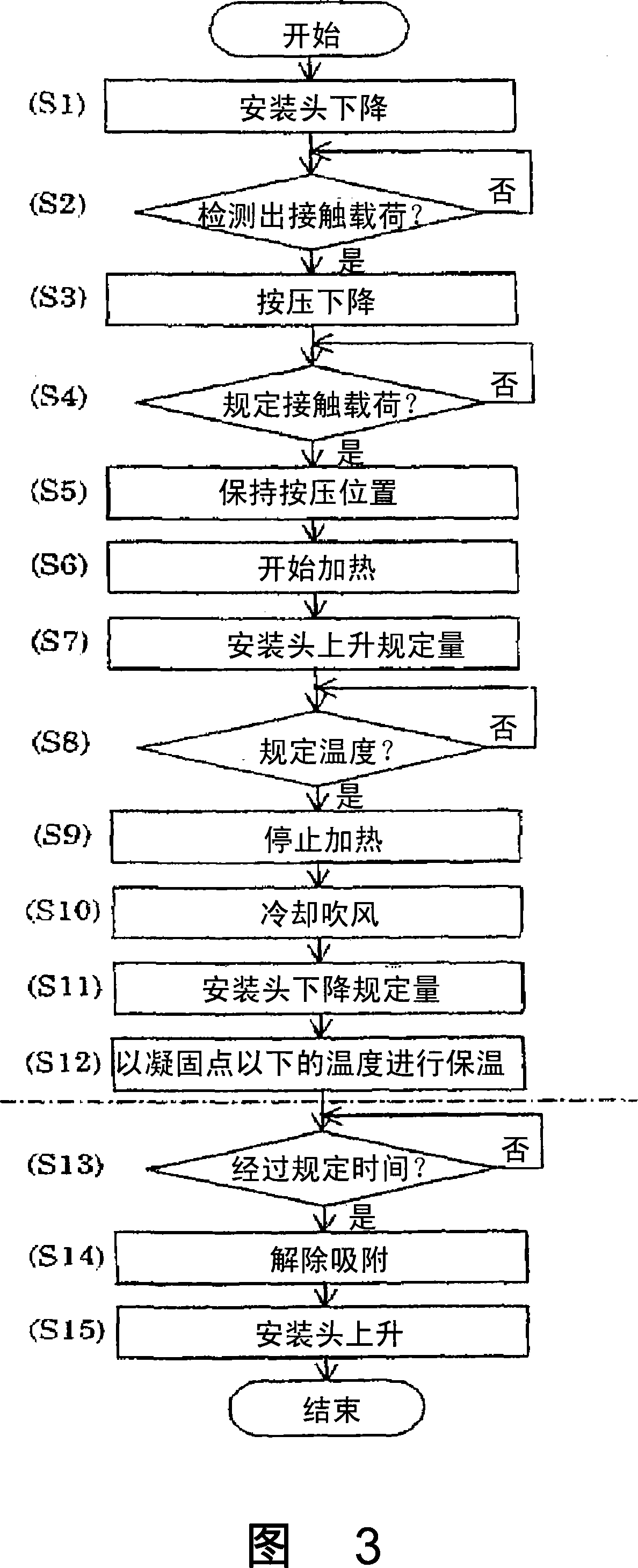
[0046] This embodiment shows how to mount an IC chip on a substrate by fusing and bonding the electrode of an IC chip as an example of an electronic component into a solder bump as a protruding electrode and forming a pad as a substrate electrode with an electrode of a substrate. The component installation method and component installation device on the above. In particular, it is a mounting control method and device thereof capable of mounting with high precision even IC chips whose planarity tends to be impaired due to thinning or IC chips in which a plurality of electrodes are arranged in a row at a narrow pitch. In addition, the object to mount the IC chip is set as the board, but it is not only the circuit board, and in the case of chip-on-chip mounting the IC chip on the IC chip, the IC chip to be mounted is set as the board.

[0047] FIG. 1 shows the main configuration of the mounting device according to the embodiment, and shows the components of the mounting head 3 th...


PUM


Abstract

There has been a possibility of deteriorating planarity of a thin IC chip due to process distortion and deformation generated when sucking the IC chip by a suction nozzle. The deformation is corrected by pressing the thin IC chip on a board (4) with a prescribed load by a suction nozzle (11) having a suction plane (11b) formed flat. A reduction of a prescribed opposing interval between the IC chip and the board (4), due to thermal expansion caused by heat applied for melting a solder bump (1a) formed on an electrode, is corrected by controlling rising of the suction nozzle (11). A peeling action of the melting part, due to a part which has heat- expanded and contracted by cooling, is corrected by controlling descending of the suction nozzle (11). Thus, an electronic component mounting method and an electronic component mounting apparatus are provided for correctly mounting even the electronic components, such as the thin IC chip easily deformed and the IC chip wherein a multitude of electrodes are formed at a narrow pitch.

Description

technical field [0001] The present invention relates to a mounting method and device for mounting electronic components on a substrate as a mounting object by using a flip-chip mounting method, and particularly relates to electronic components such as thin IC chips or IC chips in which a plurality of electrodes can be formed at narrow pitches , A component mounting method and a component mounting device that are mounted on a substrate with high precision. Background technique [0002] As one of the technologies supporting the remarkable progress in weight reduction, thinning, and high performance of portable information devices such as notebook computers and mobile phones, there is high-density mounting technology. With the development of high-density integration of IC chips, the number of electrodes serving as external connection terminals increases and is formed at a finer pitch. In order to mount the IC chip, and to prevent short circuits and poor connections to the elect...

Claims


Application Information

Patent Timeline
Patent Type & Authority Applications(China)
IPC IPC(8): H01L21/60H05K3/34H05K13/04
CPCH05K2203/0195H01L2924/01082H01L2924/0105H01L24/81H01L2924/01004H01L2224/755H01L2224/75743H05K3/3436H01L2924/3511H01L2224/81801H05K2203/0278H01L2924/14H01L2224/75745H01L2924/01005H01L2924/01033H01L2924/01006H01L2224/75H01L2924/014H01L24/75H01L2224/75502Y02P70/50
Inventor 上野康晴森川诚平田修一小林大范仕田智
Owner PANASONIC CORP
Why Eureka
Try Eureka