
Glass substrate optical display infra-red sensor
An infrared sensor, glass substrate technology, applied in the field of sensing elements, can solve the problems of reducing infrared detection sensitivity, micro-beam reflector jitter, optical readout noise, etc., to avoid infrared energy loss, eliminate thermal crosstalk, and eliminate frame structure. Effect
- Summary
- Abstract
- Description
- Claims
- Application Information
AI Technical Summary
Problems solved by technology
Method used
Image

Examples
Embodiment 1
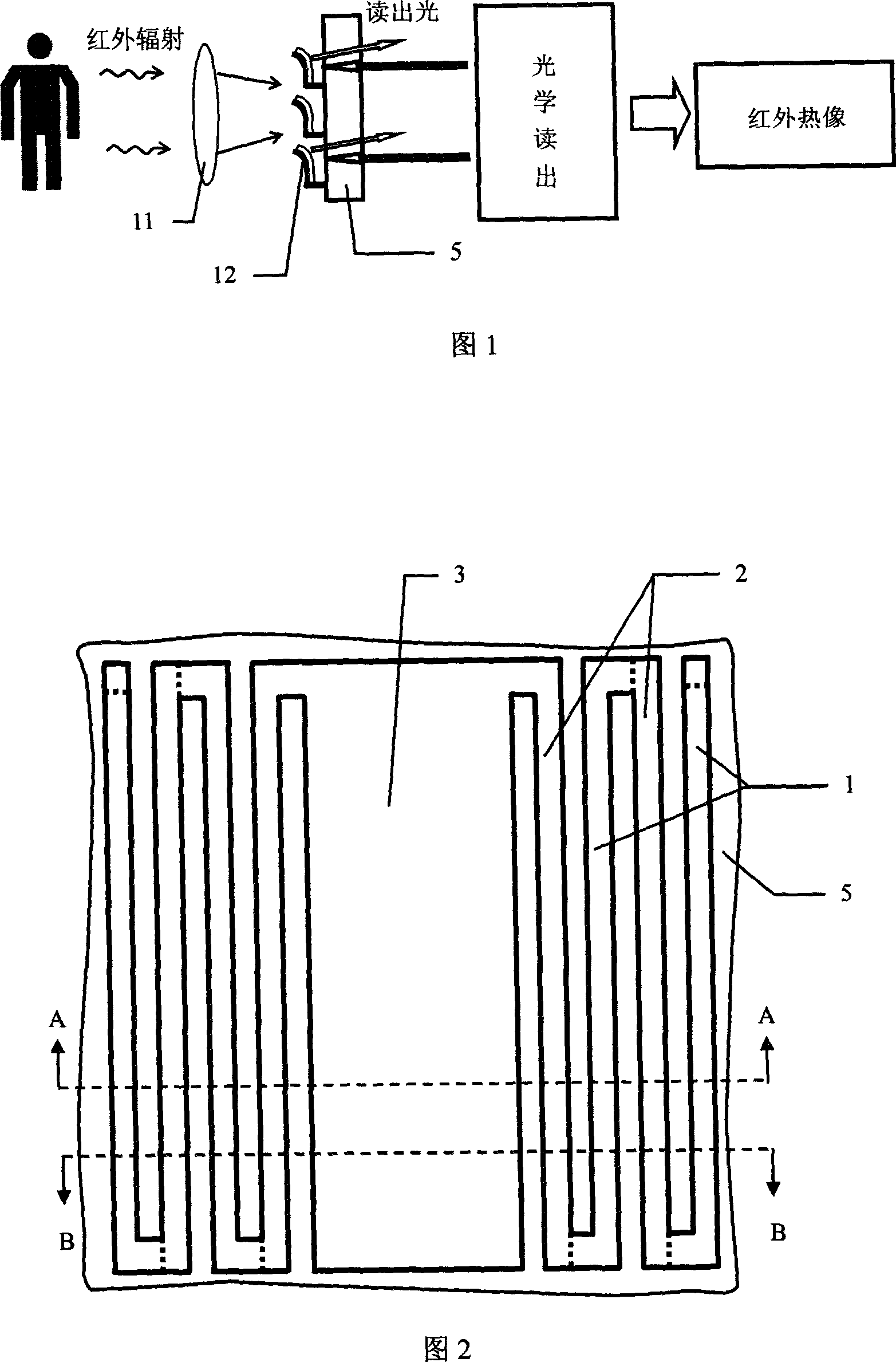
[0048] Referring to Fig. 1, Fig. 2, Fig. 3, Fig. 4 and Fig. 5, a glass substrate 5 that is transparent to visible light but not infrared is adopted, and a microbeam unit 12 with a lateral support planar structure is arranged on the glass substrate 5; the microbeam unit 12 Contains thermal deformation mechanism and infrared absorbing plate 3.
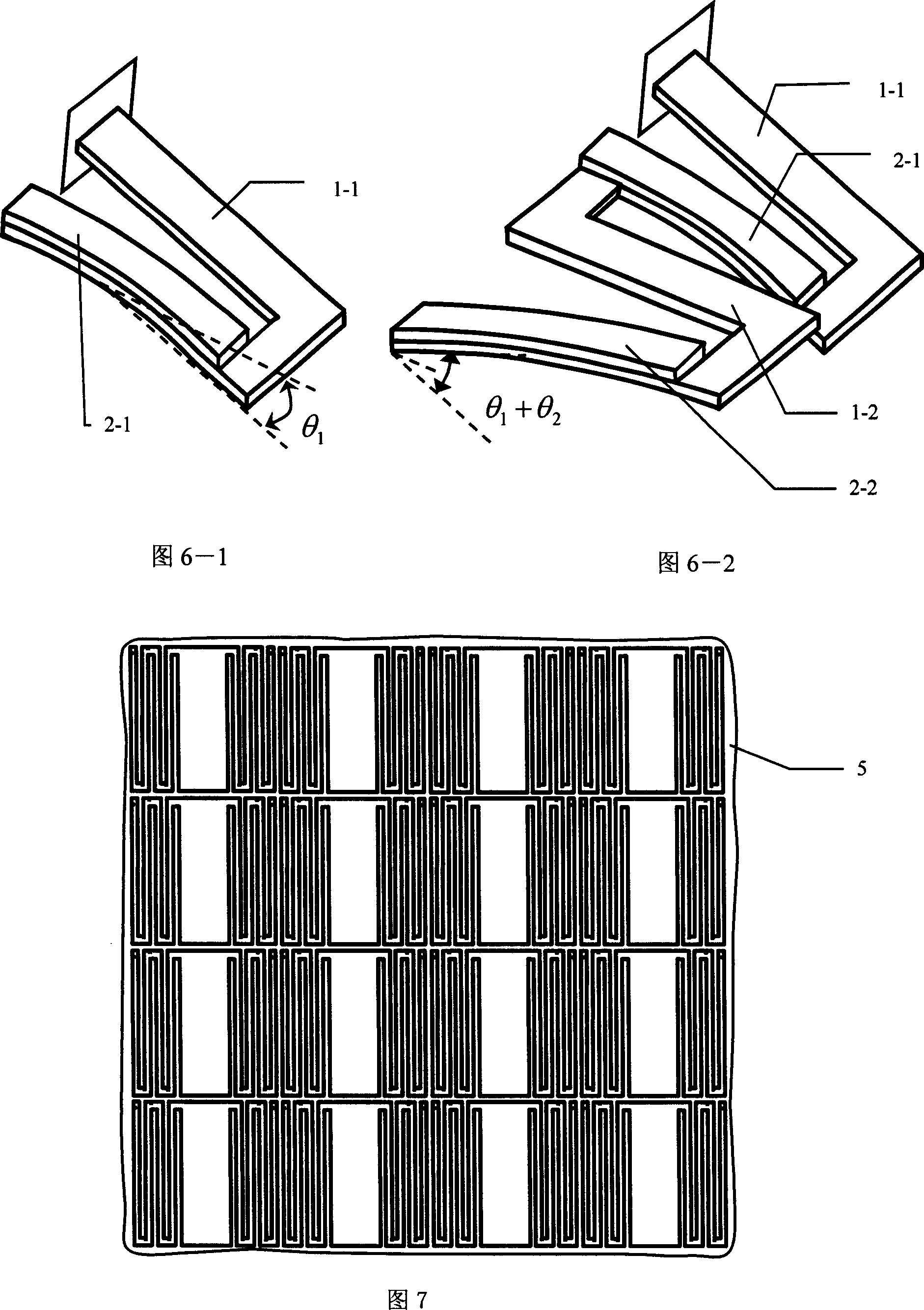
[0049] As shown in FIG. 2 , there are two groups of thermal deformation mechanisms, which are symmetrically arranged on both sides of the infrared absorbing plate 3 , and each group of thermal deformation mechanisms consists of at least one thermal isolation beam 1 and at least one thermal deformation beam 2 to form a folding distribution.
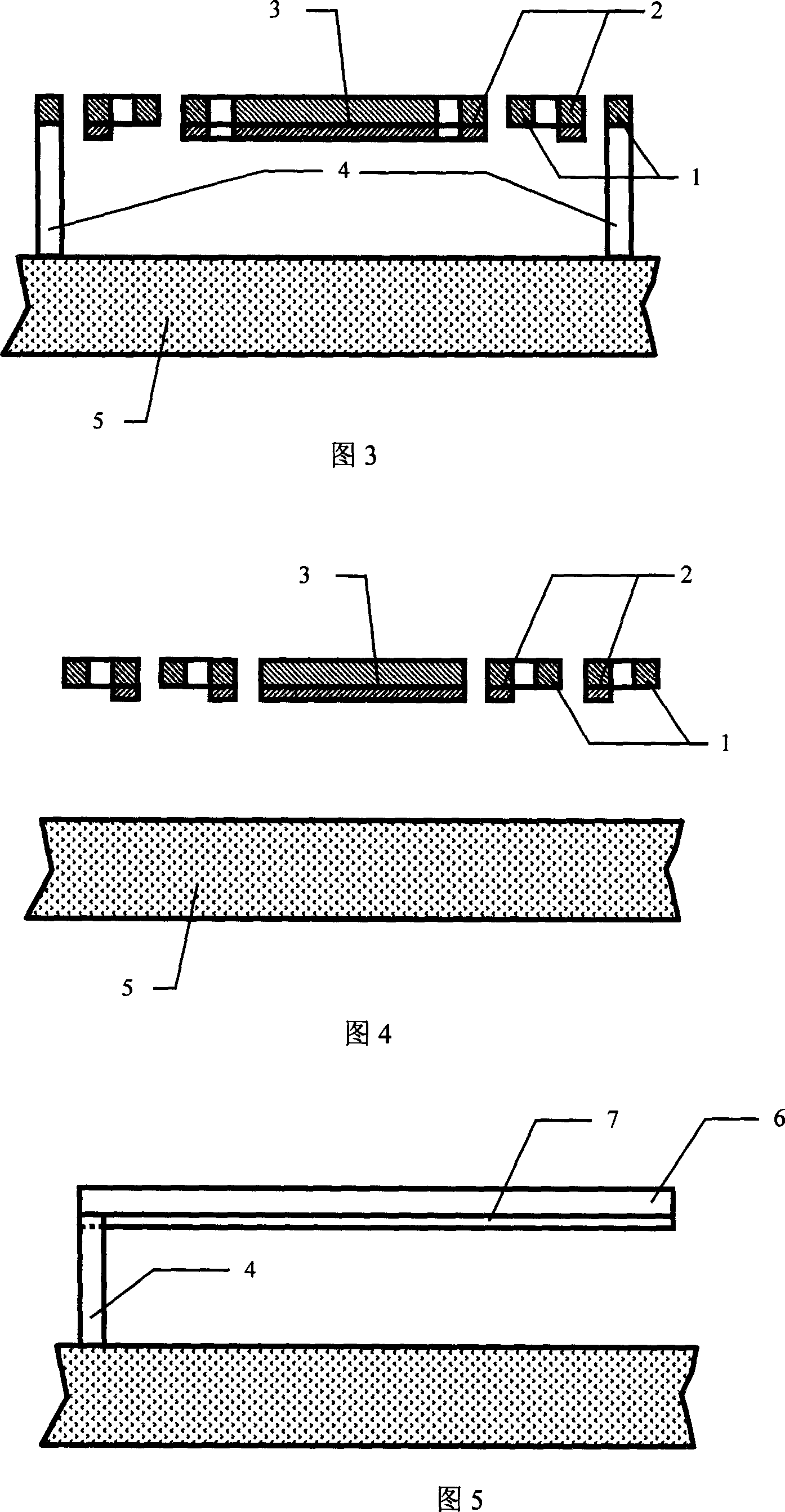
[0050] As shown in FIG. 3 , the thermal deformation mechanism is connected to both sides of the infrared absorbing plate 3 with its inner end, and its outer final beam end is fixed on the glass substrate 5 in a standing form through anchor feet 4 .
[0051] As shown in Figure 3, Figure 4 and Figure 5...
Embodiment 2
[0062] Referring to Fig. 12, Fig. 13 and Fig. 14, the difference from the above-mentioned embodiment 1 is that in this embodiment, the infrared absorbing plate adopts a double-layer structure, and the heat-absorbing resonant cavity is formed by the lower reflective plate and the upper heat-absorbing resonant plate 8 , between the reflective plate and the heat-absorbing resonant plate are connected by ribs 9, and the distance between them is , where λ is the peak value of the detected infrared wavelength, and n is a positive integer.
[0063] In specific implementation, the thickness of the lower reflective plate and the upper heat-absorbing resonant plate 8 is 0.3-3um, the thickness of the thermal isolation beam 1 and the thermal deformation beam 2 is 0.2-3um, and the distance between the micro-beam unit 12 and the glass substrate 5 is 2-3um. 7um.
[0064] In this structural form, the lower surface of the lower reflective plate is a reflective surface for optical readout det...
Embodiment 3
[0066] Referring to Fig. 15, Fig. 16 and Fig. 17, the difference from the above-mentioned embodiment 2 is that in this embodiment, on both sides of the upper heat-absorbing resonant plate 8, an eave structure is extended to increase the duty cycle of the heat-sensitive unit, The eaves just cover the area where the thermal deformation mechanism is located. The eaves structure of the heat-absorbing resonant plate 8 can increase the duty cycle of the unit, thereby improving the absorption efficiency of infrared rays and improving the detection sensitivity.
[0067] In the above-mentioned embodiments, the infrared absorbing plate 3 is made of a thin film material that has a strong absorption effect on infrared rays, such as SiN x , SiO 2 , made of polysilicon, etc., the absorption area should be as large as possible to increase the heat absorbed. Moreover, in the sensitive direction of angular deflection, the optical detection sensitivity is directly proportional to the length o...
PUM
 Abstract
Description
Claims
Application Information