Directly electric connected crystal covered encapsulation structure of semiconductor chip

An electrical connection, flip chip packaging technology, applied in the direction of semiconductor devices, semiconductor/solid-state device components, circuits, etc., can solve the problems of unstable electrical, mechanical and physical quality, high packaging cost, long production cycle, etc. Achieve the effect of improving heat dissipation efficiency, improving electrical quality, and reducing overall height

Active Publication Date: 2007-05-30
PHOENIX PRECISION TECH CORP
View PDF1 Cites 1 Cited by
  • Summary
  • Abstract
  • Description
  • Claims
  • Application Information

AI Technical Summary

Problems solved by technology

[0007] However, the manufacturing process of the flip-chip ball grid array package, the process of electrically connecting the chip packaging substrate 12 and the semiconductor chip 10 to the chip packaging substrate 12 and packaging is a separate production mode, that is, the chip packaging substrate 12 is an independent manufacturing process. The packaging of the semiconductor chip 10 to the chip packaging substrate 12 is another independent process. The two independent processes will cause problems of low yield and long production cycle. After the electrical function is improved to a certain level, it cannot be effectively improved.
Although the flip-chip ball grid array (FCBGA) structure can be used in products

Method used


Image

  • Directly electric connected crystal covered encapsulation structure of semiconductor chip
  • Directly electric connected crystal covered encapsulation structure of semiconductor chip
  • Directly electric connected crystal covered encapsulation structure of semiconductor chip

Examples


Embodiment 1

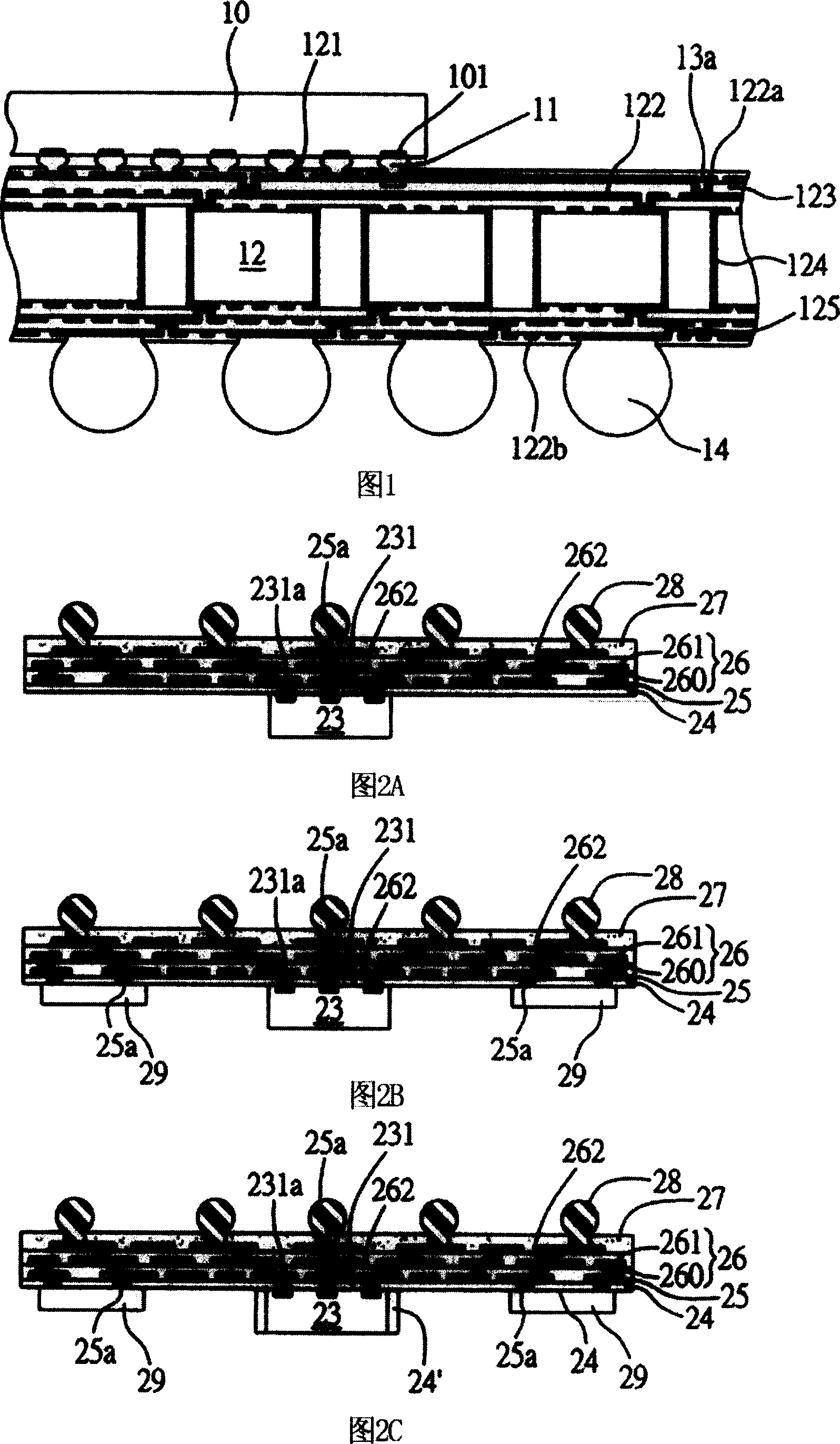
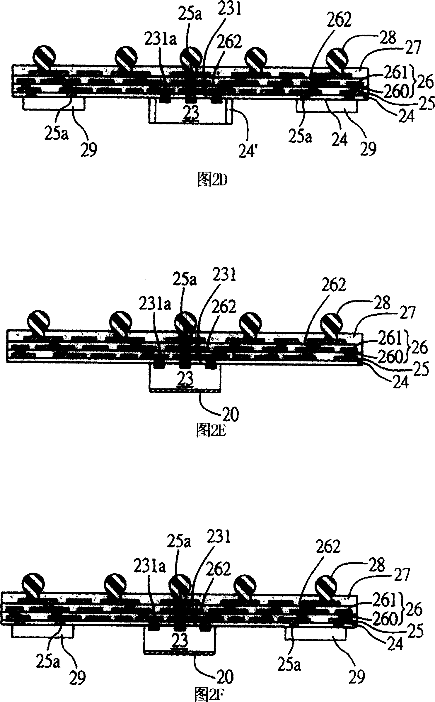
[0022] 2A to 2D are schematic cross-sectional views of Embodiment 1 of the direct electrical connection flip-chip package structure of the semiconductor chip of the present invention. One point to be noted here is that these drawings are simplified schematic diagrams, which only illustrate the basic structure of the present invention in a schematic manner, so only the structures related to the present invention are shown, and the shown structures are not the number of actual implementations , shape and size ratio, the number, shape and size ratio in actual implementation is a selective design, and its composition and layout may be more complex.

[0023] The direct electrical connection flip-chip packaging structure of the semiconductor chip of the present invention shown in FIG. 2A includes: at least one semiconductor chip 23, the semiconductor chip has an active surface 231 and a non-active surface, and the active surface 231 of the semiconductor chip 23 forms There is an ele...

Embodiment 2

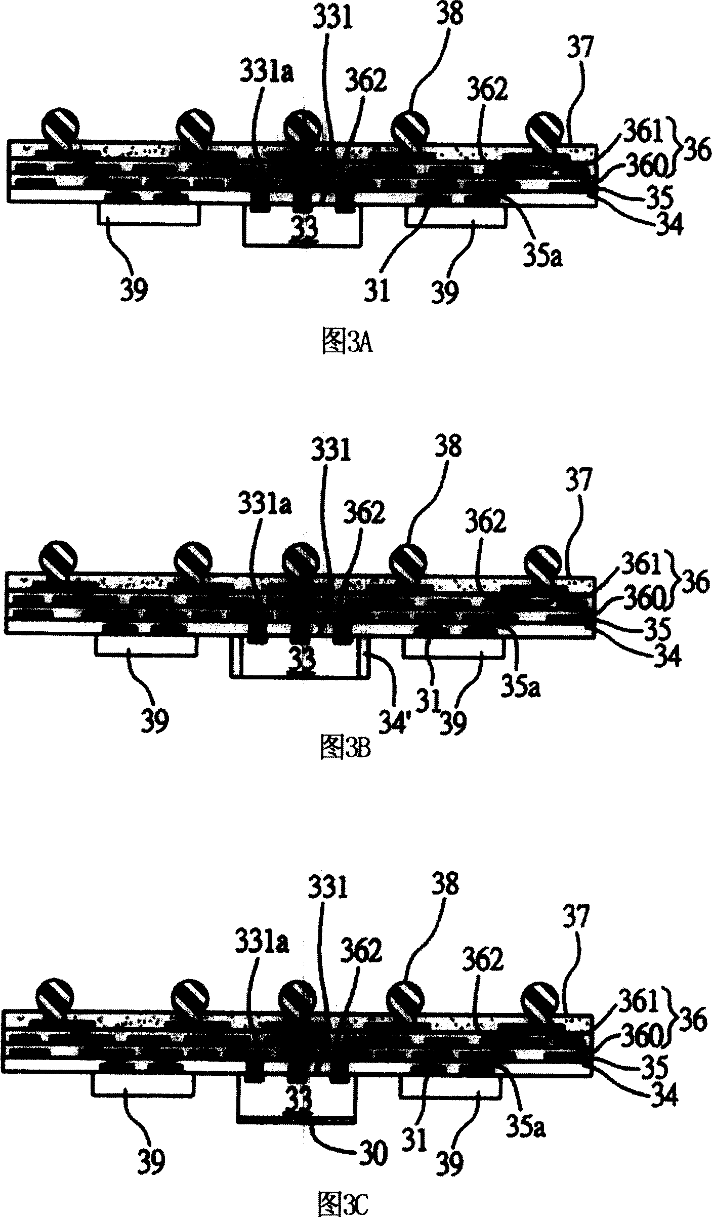
[0033] Please also refer to FIG. 3A to FIG. 3C , which are schematic cross-sectional views of Embodiment 2 of the direct electrical connection flip-chip package structure of the semiconductor chip of the present invention. Embodiment 2 of the present invention is similar to Embodiment 1, and the main difference is that an electrode pad is formed on the lower surface of the dielectric layer, so that the semiconductor chip and the electrode pad are exposed to the outside, reducing the overall height of the structure, and realizing the purpose of lightness, thinness and shortness. And because it has electrode pads, it can further provide electrical connection to external electronic components.

[0034] Please refer to FIG. 3A, the semiconductor chip direct electrical connection flip-chip packaging structure of the present invention includes: at least one semiconductor chip 33, and the active surface 331 of the semiconductor chip 33 is formed with an electrical connection pad 331a;...


PUM


Abstract

This invention relates to semiconductor chip direct electricity connection with film sealing structure, which comprises the following parts: at least one dielectric layer; at least one semiconductor chip with connection pad by main surface set on the dielectric layer; at least one circuit layer formed on the dielectric layer on one side of chip; conductor electrode formed on dielectric layer; electricity connection pad to semiconductor chip.

Description

technical field [0001] The invention relates to a direct electrical connection flip-chip packaging structure of a semiconductor chip, in particular to a direct electrical connection flip-chip packaging structure of an integrated semiconductor chip and a thinned semiconductor chip. Background technique [0002] With the vigorous development of the electronic industry, electronic products have gradually entered the direction of multi-functional and high-performance research and development. In order to meet the packaging requirements of high integration and miniaturization of semiconductor packages, circuit boards that provide multiple active and passive components and line connections have gradually evolved from single-layer boards to multi-layer boards ( Multi-layer bord), in a limited space, uses the interlayer connection technology to expand the available wiring area on the circuit board to meet the needs of high-density integrated circuits (Integrated circuit). [0003] ...

Claims


Application Information

Patent Timeline
IPC IPC(8): H01L23/498H01L23/50
CPCH01L24/19H01L2224/04105H01L2224/12105H01L2224/16227H01L2224/19H01L2224/20H01L2224/24195H01L2224/73267H01L2924/14H01L2924/19105H01L2924/00H01L2924/00012
Inventor 许诗滨
Owner PHOENIX PRECISION TECH CORP
Why Eureka
Try Eureka