
Eureka
For R&D, Eureka makes reading and utilizing patents & technical documents easy.
Eureka AIR
Designed for self-driven R&D workflows. Generate viable solutions, solve complex R&D challenges, empower your innovation with AI.

Eureka Materials
Designed for material experts only. Revolutionize your material R&D, from search, analyze, to developing new materials.

TechResearch
Generate reliable direction feasibility study reports for your R&D in just a few steps.

TechSeek
Discover and master advanced knowledge NOW. Basics, ideas, possibilities, all at once.

TechMind
As an expert in R&D Theories, TechMind can generates customized viable solutions instantly.

TechRisk
Analyze your overall solution with one click, know your potential R&D risks in advance.

TechMonitor
Get weekly tech updates, stay abreast of the latest tech innovations and key insights.
Organic bistable element and its manufacturing method
A manufacturing method and bistable technology, applied in semiconductor/solid-state device manufacturing, electrical components, electric solid-state devices, etc., can solve problems affecting component life, multi-stable layer damage, limited application level, etc., to improve life, Effect of increasing write/erase times
- Summary
- Abstract
- Description
- Claims
- Application Information
AI Technical Summary
Problems solved by technology
Method used
Image

Examples
Embodiment Construction
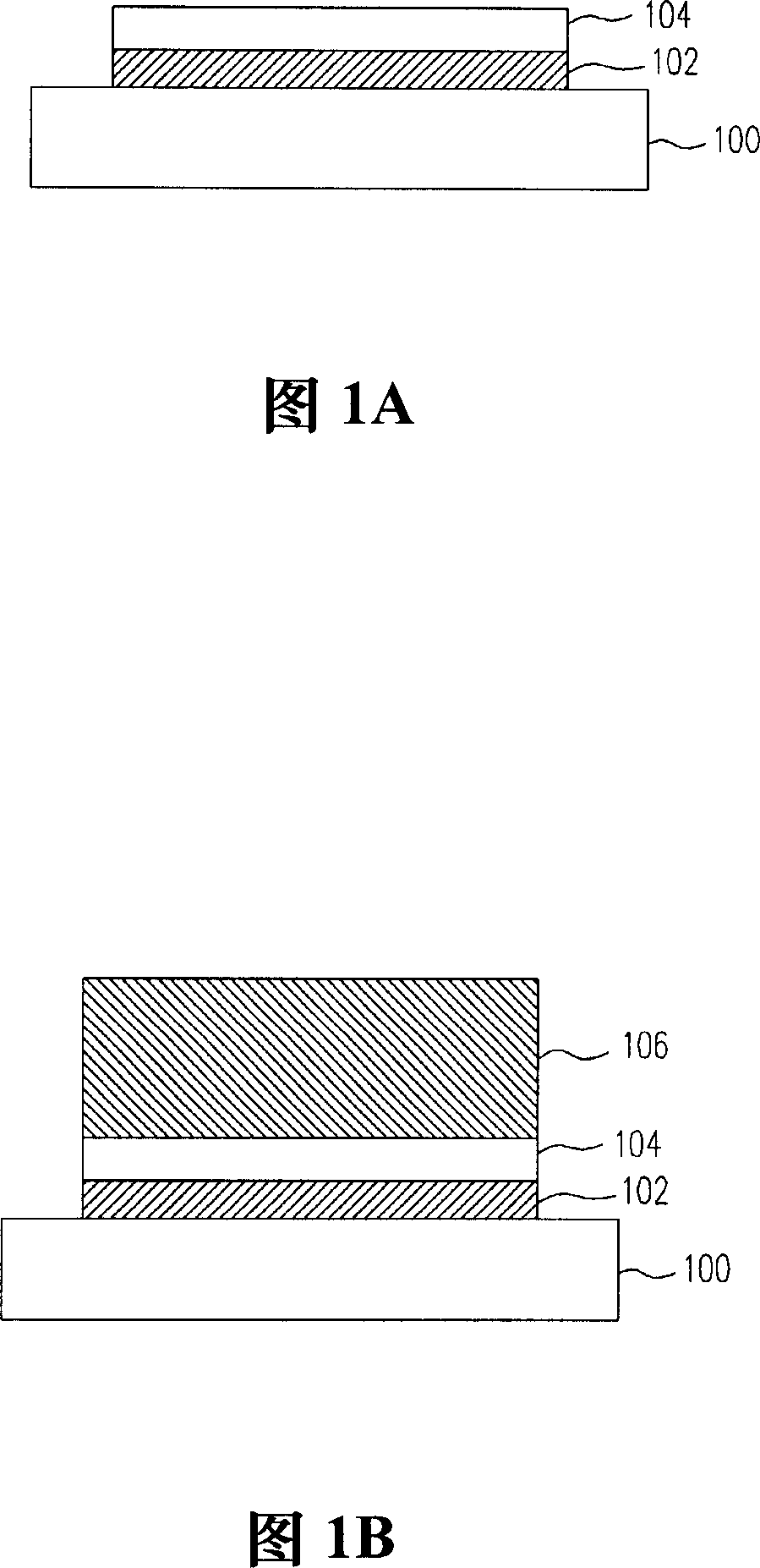
[0050] 1A to 1C are cross-sectional views of a method for manufacturing an organic bistable device according to a preferred embodiment of the present invention.
[0051] Referring to FIG. 1A , a substrate 100 is provided. A first metal layer 102 is formed on the substrate 100 . The material of the first metal layer 102 is copper, gold, silver, aluminum, cobalt or nickel, and the thickness of the first metal layer 102 is about 700 angstroms. Afterwards, a buffer layer 104 is formed on the first metal layer 102 . Wherein the buffer layer 104 is formed by, for example, a material with a high dielectric constant, and the material with a high dielectric constant is preferably Al 2 o X , LiF, MgO, V 2 o 5 or TiO 2 . Also, the thickness of the buffer layer 104 is about 40 angstroms.
[0052]Next, please refer to FIG. 1B , an organic mixed layer 106 is formed on the buffer layer 104 . Wherein, the method for forming the organic mixed layer 106 includes performing a jet printi...
PUM
| Property | Measurement | Unit |
|---|---|---|
| thickness | aaaaa | aaaaa |
Abstract
Description
Claims
Application Information
 - R&D Engineer
- R&D Manager
- IP Professional
- Industry Leading Data Capabilities
- Powerful AI technology
- Patent DNA Extraction
Browse by: Latest US Patents, China's latest patents, Technical Efficacy Thesaurus, Application Domain, Technology Topic, Popular Technical Reports.
© 2024 PatSnap. All rights reserved.Legal|Privacy policy|Modern Slavery Act Transparency Statement|Sitemap|About US| Contact US: help@patsnap.com