Method for manipulating microscopic particles and analyzing the composition thereof

A particle and sample technology, used in the field of semiconductor sample surface removal and analysis of tiny particles, which can solve problems such as reducing the cycle time of pollutant removal

Inactive Publication Date: 2007-06-06
OMNIPROBE
View PDF0 Cites 13 Cited by
  • Summary
  • Abstract
  • Description
  • Claims
  • Application Information

AI Technical Summary

Problems solved by technology

In-line process using existing manufacturing and testing equipment dramatically reduces cycle time for contaminant removal

Method used


Image

  • Method for manipulating microscopic particles and analyzing the composition thereof
  • Method for manipulating microscopic particles and analyzing the composition thereof
  • Method for manipulating microscopic particles and analyzing the composition thereof

Examples


Embodiment Construction

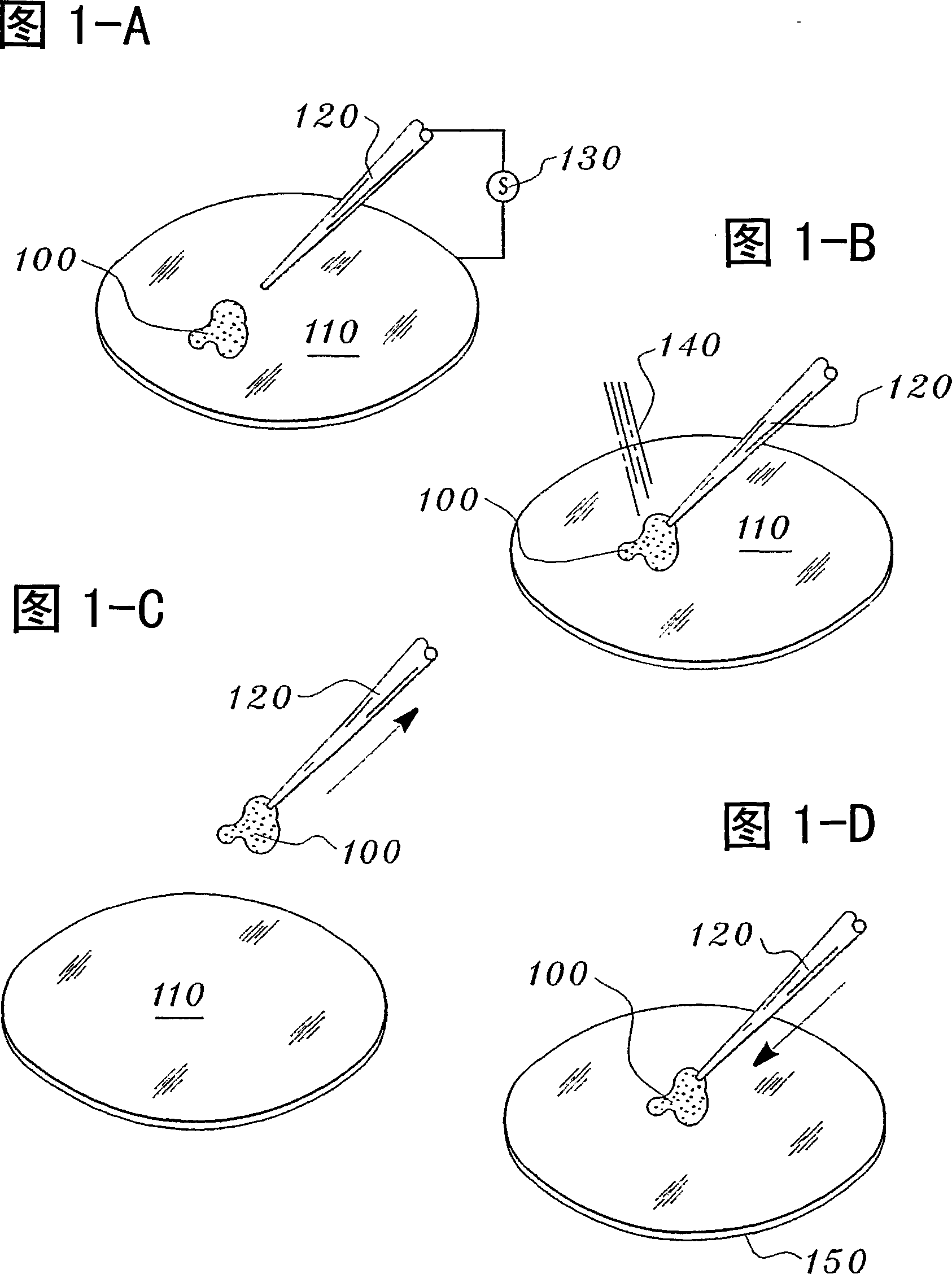
[0024]Semiconductor manufacturing typically uses scanning electron microscopes (SEM), focused ion beam (FIB) instruments, or scanning Auger microprobes (SAM) to analyze tiny particles. FIB instruments are available in single-beam or dual-beam (SEM and ion beam) modes. Commonly used FIB instruments are manufactured by FEI Corporation of Hillsboro, Oregon, and there are several models of 200, 235, 820, 830 and 835. The probe 120 mentioned below is a component of the micromanipulator connected to the FIB instrument with vacuum feedthrough. A conventional such micromanipulator is the Model 100 micromanipulator manufactured by Omniprobe Corporation of Dallas, Texas. Typical SAM instruments include Peabody, JAMP-7810 and JAMP-7830F manufactured by JEOL USA, Inc. of Massachusetts.

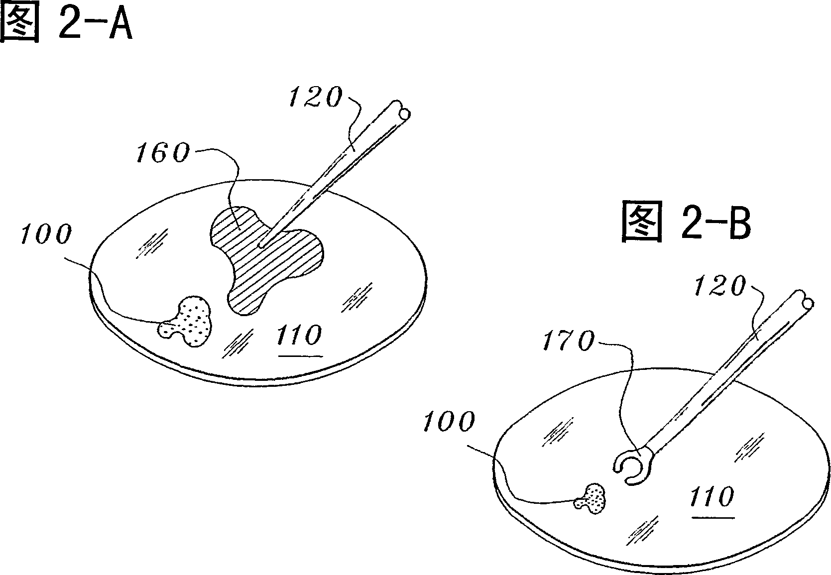
[0025] Figure 1 depicts a common setup for handling and analyzing particles. FIG. 1A shows a particle 100 to be detected resting on a first sample surface 110 . The micromanipulator probe 120 is locat...


PUM


Abstract

We disclose a method for analyzing the composition of a microscopic particle resting on a first sample surface. The method comprises positioning a micro-manipulator probe near the particle; attaching the particle to the probe; moving the probe and the attached particle away from the first sample surface; positioning the particle on a second sample surface; and, analyzing the composition of the particle on the second sample surface by energy-dispersive X-ray analysis or detection of Auger electrons. The second surface has a reduced or non-interfering background signal during analysis relative to the background signal of the first surface. We also disclose methods for adjusting the electrostatic forces and DC potentials between the probe, the particle, and the sample surfaces to effect removal of the particle, and its transfer and relocation to the second sample surface.

Description

technical field [0001] The present invention relates to a method for removing and analyzing microscopic particles from the surface of a sample, especially a semiconductor sample. Background technique [0002] In the production process of the semiconductor industry, the inevitable particle pollution will reduce the yield. As the semiconductor industry has been concentrating on dramatically reducing the feature size of patterned linewidths, the minimum particle size that degrades performance has also rapidly decreased. It is generally believed that a reasonable estimate of the size of a "fatal defect" on a semiconductor wafer should be greater than one third of the smallest feature size. [0003] Although semiconductor manufacturing takes place in cleanrooms with stringent particle standards, contamination is unavoidable due to movement of objects, people entering and exiting, gas condensation, and room aging. Controlling and removing these particles is an ongoing process. ...

Claims


Application Information

Patent Timeline
Patent Type & Authority Applications(China)
IPC IPC(8): G01N23/22G01N1/28B01D59/44G02B21/32
CPCG02B21/32H01J2237/31745G01N23/2204
Inventor 托马斯·M·穆尔约翰·M·安东尼
Owner OMNIPROBE
Why Eureka
Try Eureka