Safety detecting method for system integrated chip with built-in non-volatile memory

A non-volatile memory and system integration technology, applied in static memory, semiconductor/solid-state device testing/measurement, electronic circuit testing, etc., can solve problems such as low security, inflexible application, and inability to re-enter test mode. Achieve high security and ensure data security

Inactive Publication Date: 2007-06-13
SHANGHAI HUA HONG NEC ELECTRONICS
View PDF0 Cites 10 Cited by
  • Summary
  • Abstract
  • Description
  • Claims
  • Application Information

AI Technical Summary

Problems solved by technology

[0006] The above scheme of implementing chip security testing by changing the physical connection has the following problems: the physical change method is a destructive method, and the test mode cannot be re-entered after the change, and the application is not flexible; the user may realize the re-entry of the test mode through a physical repair method , and obtain circuit data information, the security is not high

Method used


Image

  • Safety detecting method for system integrated chip with built-in non-volatile memory

Examples


Embodiment Construction

[0011] The present invention will be described in further detail below in conjunction with the accompanying drawings.

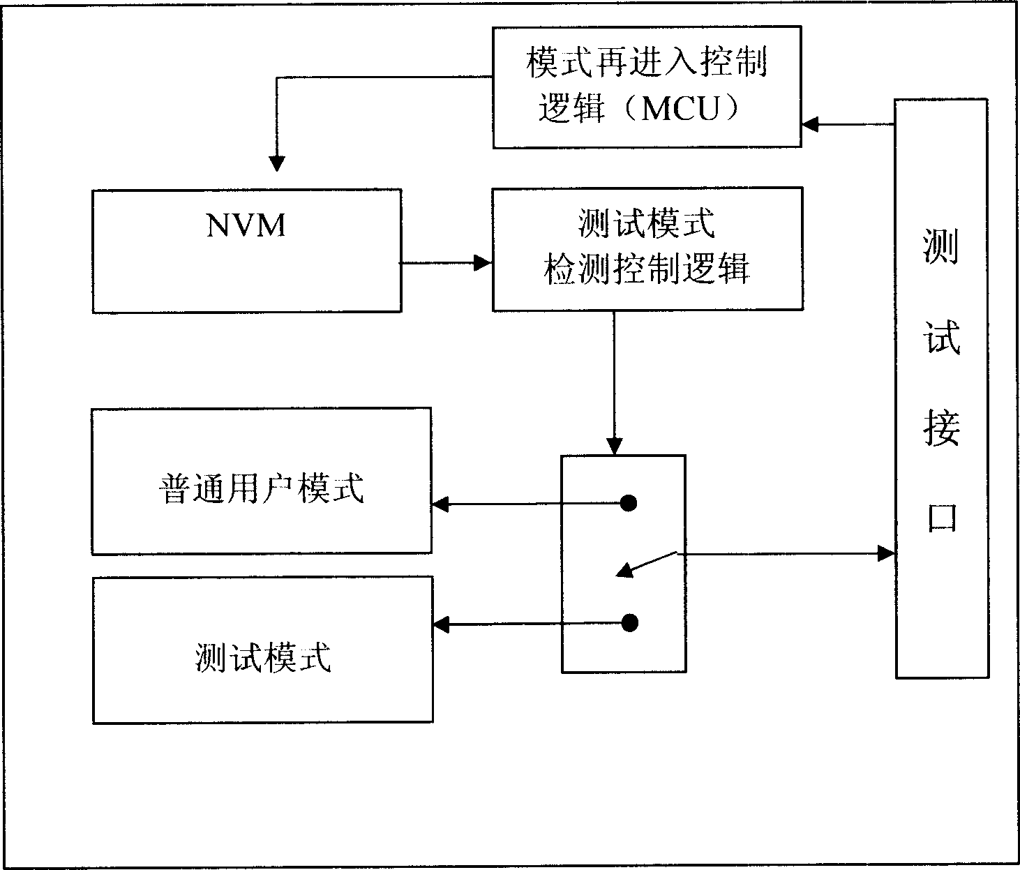
[0012] The NVM embedded in the SOC chip, such as flash memory (Flash), electrically erasable programmable read-only memory (EEPROM) etc., its data has the characteristic of power-down retention, the present invention utilizes this characteristic to carry out between test mode and user mode switch.

[0013] Referring to the accompanying drawings, the present invention sets a test mode detection control logic, which realizes the switching of the test mode based on the judgment of the data of the embedded NVM specific address, which is inaccessible in the user mode. In the initial state after the chip is manufactured, since the data at the specific address of the NVM is non-specified data, the chip is in the test mode state, and the internal module test can be realized directly through the chip pins. When the test is completed, the specified mode setting data i...


PUM


Abstract

The invention discloses a safe test method for an SOC (system on chip) embedded with nonvolatile memory (NVM), detecting data at embedded NVM specific addresses by a test mode detecting logic so as to implement test mode switching, where the embedded NVM specific addresses can not be accessed in user mode, and when the test is finished, it writes the appointed mode setting data at the embedded NVM specific addresses, and after detecting the data, a test mode logic circuit of the SOC intermediately switches the chip to the user mode to cut off test circuits of internal modules so as to make the chip enter into common user mode, thus implementing access inhibition to the internal modules. For reentering into the chip test mode, the invention also erases the mode setting data in the NVM by a special microprocessing instruction and simultaneously erases all data in the NVM so as to protect data.

Description

technical field [0001] The invention relates to an integrated circuit testing method, in particular to a system integrated chip safety testing method. Background technique [0002] Wafer-level testing of system integrated chip (SOC) products often involves the testing of internal logic function modules, analog IP modules and memory. Based on the protection of circuit design intellectual property rights and data security considerations, it is necessary to test The path is cut off, so that ordinary users can only use the functions in user mode, but cannot directly access the circuit modules inside the SOC and the data information in specific storage areas. Such tests are called security tests. [0003] Implementing chip security testing by changing the physical connection is a relatively common design technology at present. There are two main methods, one is fuse cutting, and the other is dicing groove cutting. [0004] The fuse cutting technology is to switch between the tes...

Claims


Application Information

Patent Timeline
Patent Type & Authority Applications(China)
IPC IPC(8): G11C29/00H01L21/66G01R31/28
Inventor 曾志敏
Owner SHANGHAI HUA HONG NEC ELECTRONICS
Why Eureka
Try Eureka