Method of manufacturing non-volatile memory element

A technology of non-volatile storage and manufacturing method, which is applied in the field of manufacturing electrically rewritable non-volatile storage elements, can solve problems such as the inability to easily realize DRAM storage capacity, and achieve the effect of enhancing heat generation efficiency

Inactive Publication Date: 2007-06-20
PS4 LUXCO SARL
View PDF1 Cites 0 Cited by
  • Summary
  • Abstract
  • Description
  • Claims
  • Application Information

AI Technical Summary

Problems solved by technology

Other non-volatile memories exist, such as magnetoresistive random access memory (MRAM) and ferroelectric random access memory (FRAM), but they cannot easily achieve the storage capacity that DRAM can achieve

Method used


Image

  • Method of manufacturing non-volatile memory element
  • Method of manufacturing non-volatile memory element
  • Method of manufacturing non-volatile memory element

Examples


Embodiment Construction

[0038] Preferred embodiments of the present invention will be described in detail below with reference to the accompanying drawings.

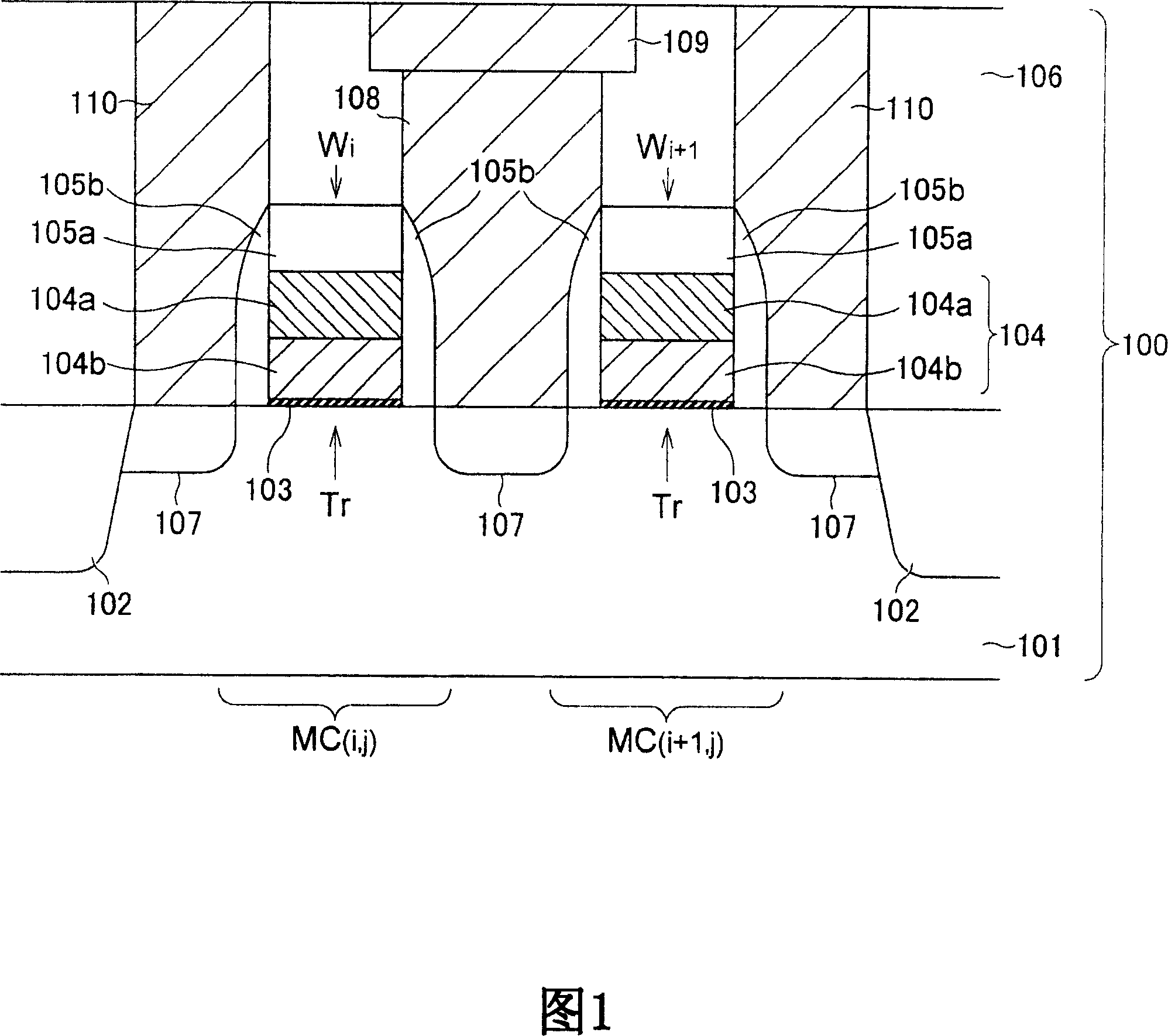
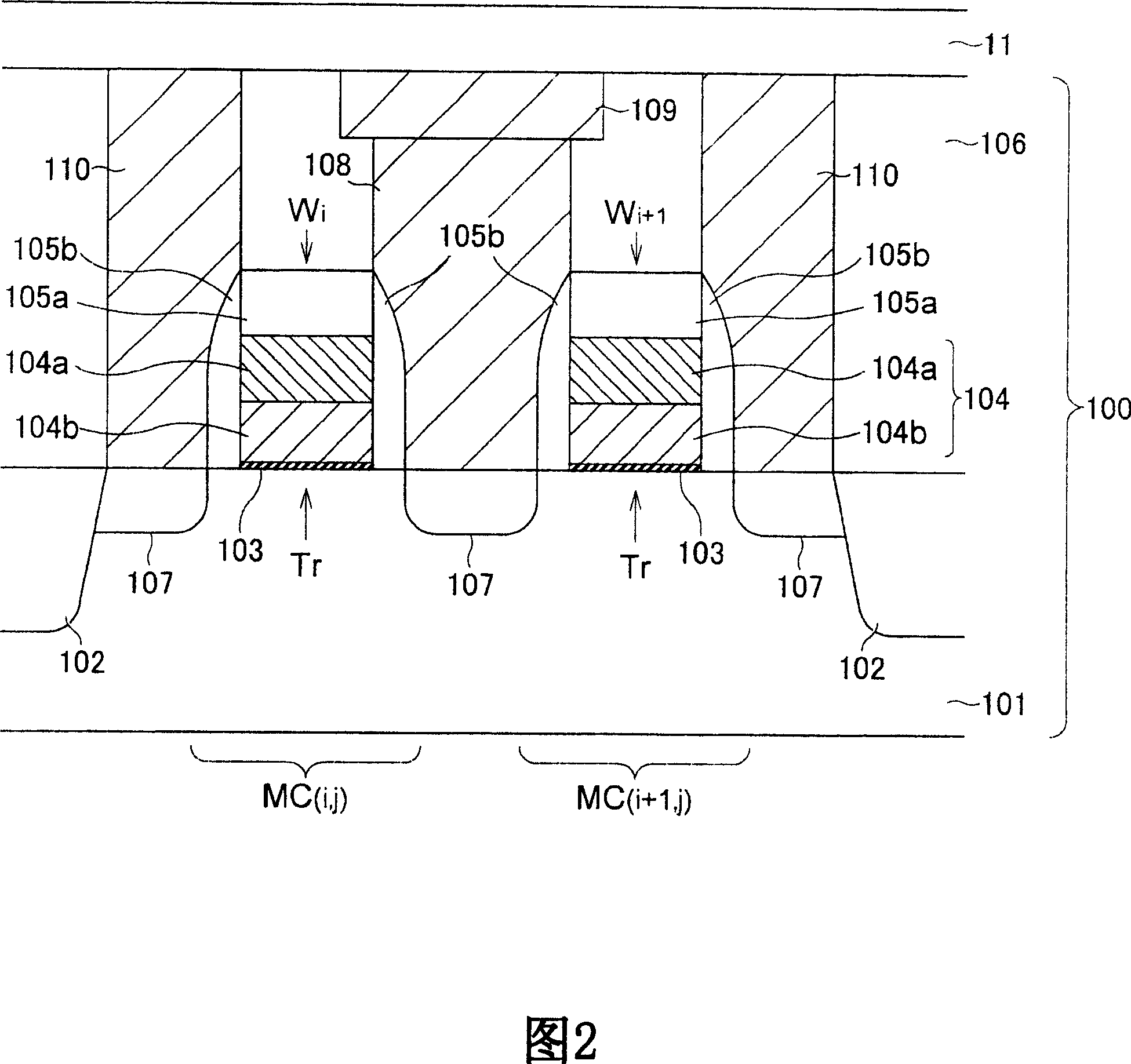
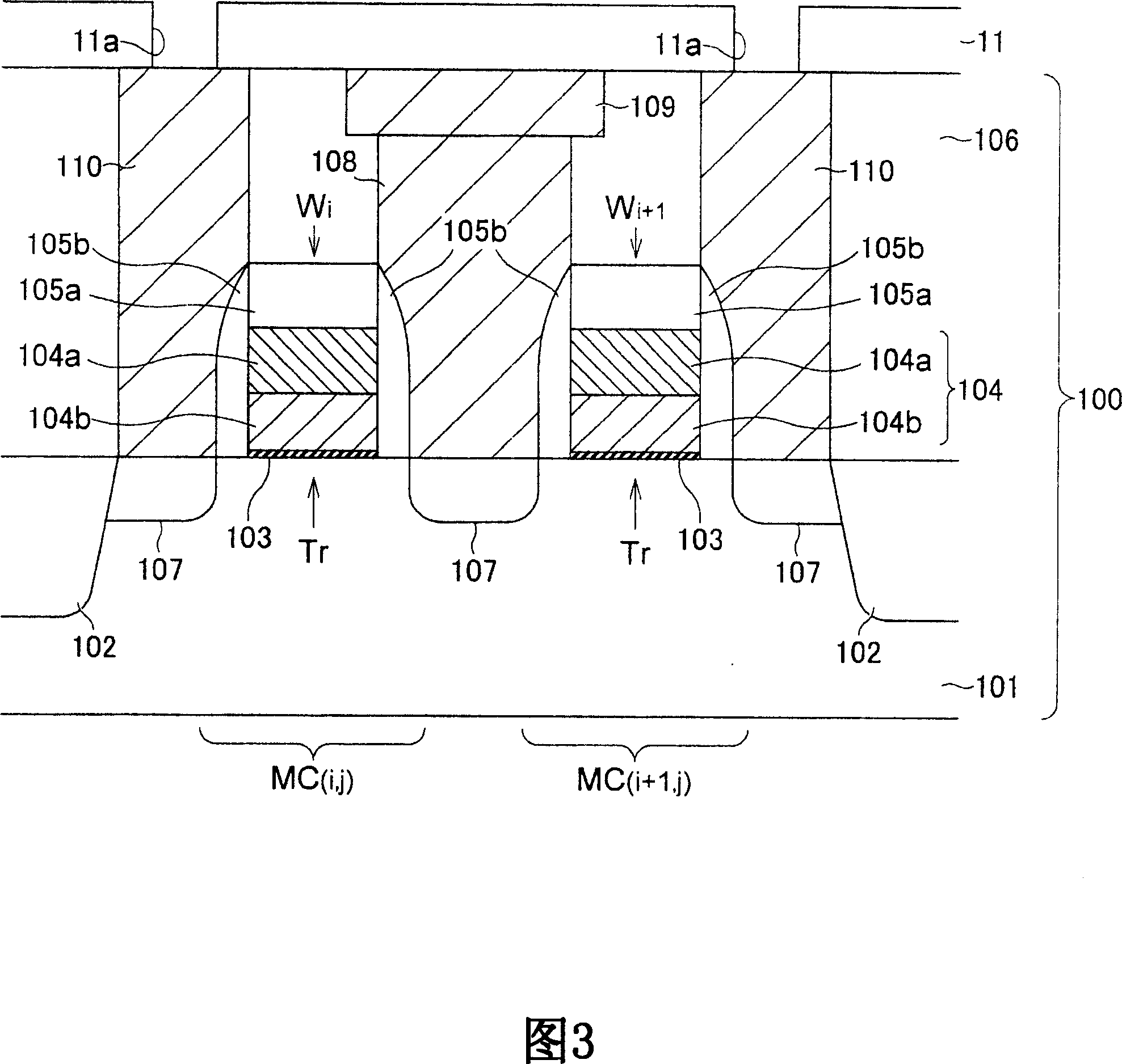
[0039] 1 to 10 are schematic cross-sectional views showing a method of manufacturing a nonvolatile memory element according to a first preferred embodiment of the present invention.

[0040] In the method of manufacturing a nonvolatile memory element according to the present embodiment, first, a transistor layer 100 is formed on a semiconductor substrate 101 (FIG. 1). The structure and method for forming the transistor layer 100 are not particularly limited, and the transistor layer 100 can be formed using known methods. The transistor layer 100 as shown has two transistors Tr. The gates 104 of the transistor Tr are respectively configured with word lines Wi and Wi+1. The gate 104 has a polycide structure composed of a polysilicon film 104 a and tungsten silicide (WSi) 104 b, and is formed on the gate insulating film 103 . The grid 104 has a...


PUM


Abstract

A method of manufacturing a non-volatile memory element in the present invention comprises a first step for forming an adhesion layer on an interlayer insulating film so that an electrical connection is established with a lower electrode, a second step for forming a recording layer containing a phase change material on the adhesion layer, a third step for forming an upper electrode that is electrically connected to the recording layer, and a fourth step for diffusing in the recording layer some of the adhesion layer positioned between at least the lower electrode and the recording layer.

Description

technical field [0001] The present invention relates to a method of manufacturing an electrically rewritable nonvolatile memory element. More specifically, the present invention relates to a method of fabricating a nonvolatile memory element having a recording layer comprising a phase change material. Background technique [0002] Personal computers and servers alike use hierarchical storage devices. There are lower-tier memories that are cheap and provide high storage capacity, and memories higher than that can provide high-speed operation. The lowest level usually consists of magnetic storage such as hard disks and tapes. In addition to non-volatile storage, magnetic storage is an inexpensive way to store information in much larger volumes than solid-state devices such as semiconductor memory. However, compared to the sequential access operation of magnetic memory devices, semiconductor memories are faster and can access stored data randomly. For these reasons, magneti...

Claims


Application Information

Patent Timeline
Patent Type & Authority Applications(China)
IPC IPC(8): H01L45/00H01L27/24G11C16/02
CPCH01L45/126H01L27/2472H01L45/148H01L45/06H01L27/2436H01L45/143H01L45/144H01L45/1625H01L45/1233H01L45/1658H10B63/30H10B63/82H10N70/231H10N70/826H10N70/8413H10N70/8825H10N70/8828H10N70/884H10N70/026H10N70/046
Inventor 川越刚浅野勇
Owner PS4 LUXCO SARL
Why Eureka
Try Eureka