Nitride semiconductor laser element and fabrication method thereof
A technology of nitride semiconductors and laser components, applied in semiconductor lasers, laser components, optical waveguide semiconductor structures, etc., can solve problems such as low yield, easy sudden breakdown, and failure to achieve optical output
- Summary
- Abstract
- Description
- Claims
- Application Information
AI Technical Summary
Problems solved by technology
Method used
Image

Examples
example 1
[0095] The structural outline of the nitride semiconductor laser element 10 of this example is shown in an external perspective view shown in FIG. 5 . The structure of this nitride semiconductor laser element 10 will be described below in the manner of its manufacturing process.
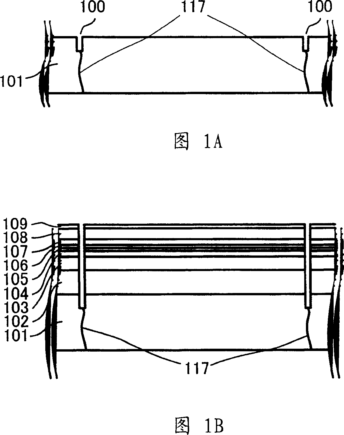
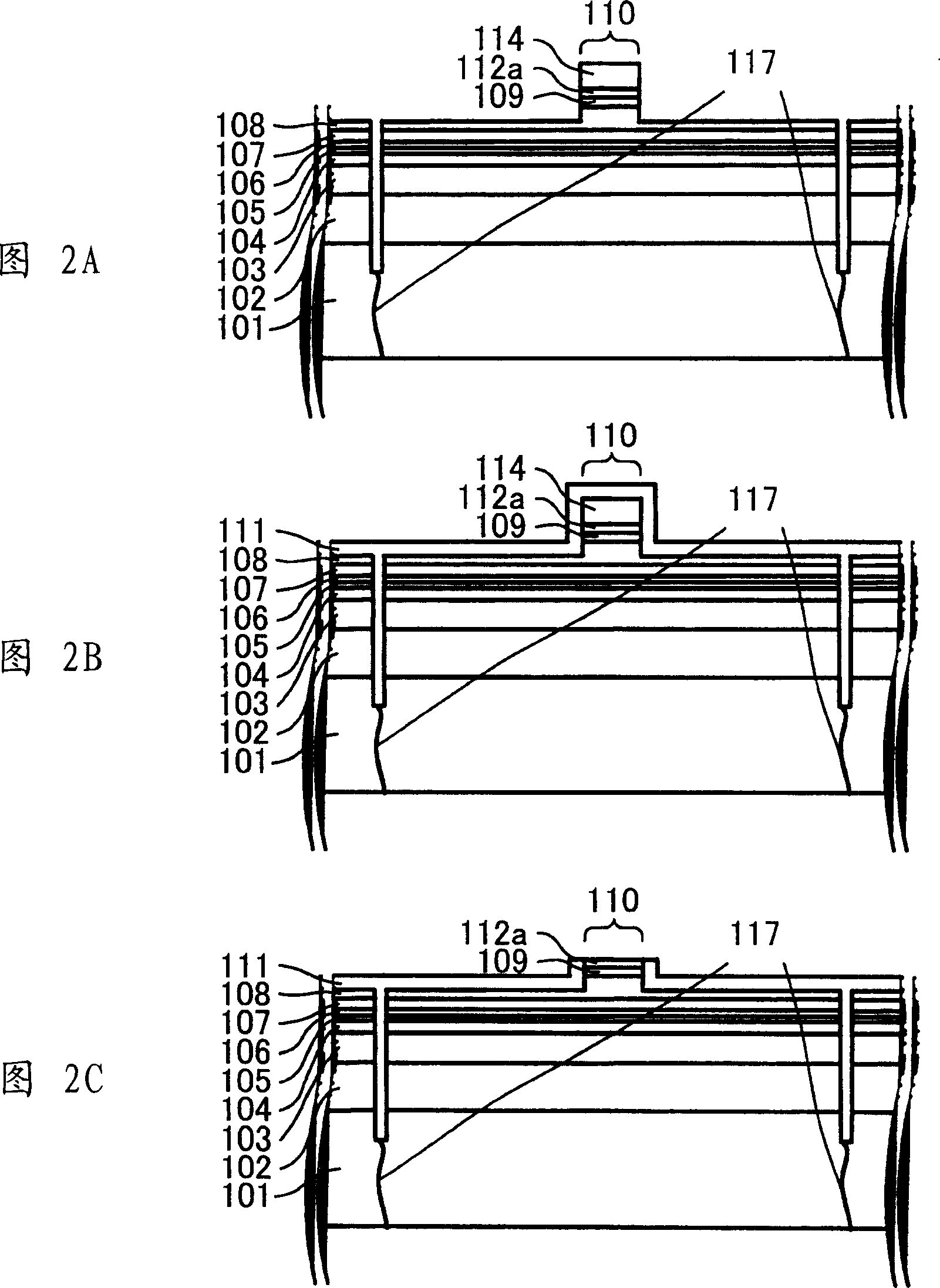
[0096] In the nitride semiconductor laser element 10 of this example, in the surface of the n-type GaN substrate 101 , grooves 100 are formed at intervals of 400 μm so as to be disposed above the defect dense regions 117 . Then, on the first main plane of the n-type GaN substrate 101 having grooves 100 formed at intervals of 400 μm, the following layers are sequentially formed: an n-type GaN lower contact layer 102 having a thickness of 2.5 μm; 3.0μm n-type Al 0.05 Ga 0.95 N lower cladding layer 103; by In x1 Ga 1-x1 N quantum well layer and In x2 Ga 1-x2 Active layer 105 composed of N barrier layers alternately arranged (where x1>x2); p-type Al with a thickness of 0.01 μm 0.3 Ga 0.7 N anti-e...
example 2
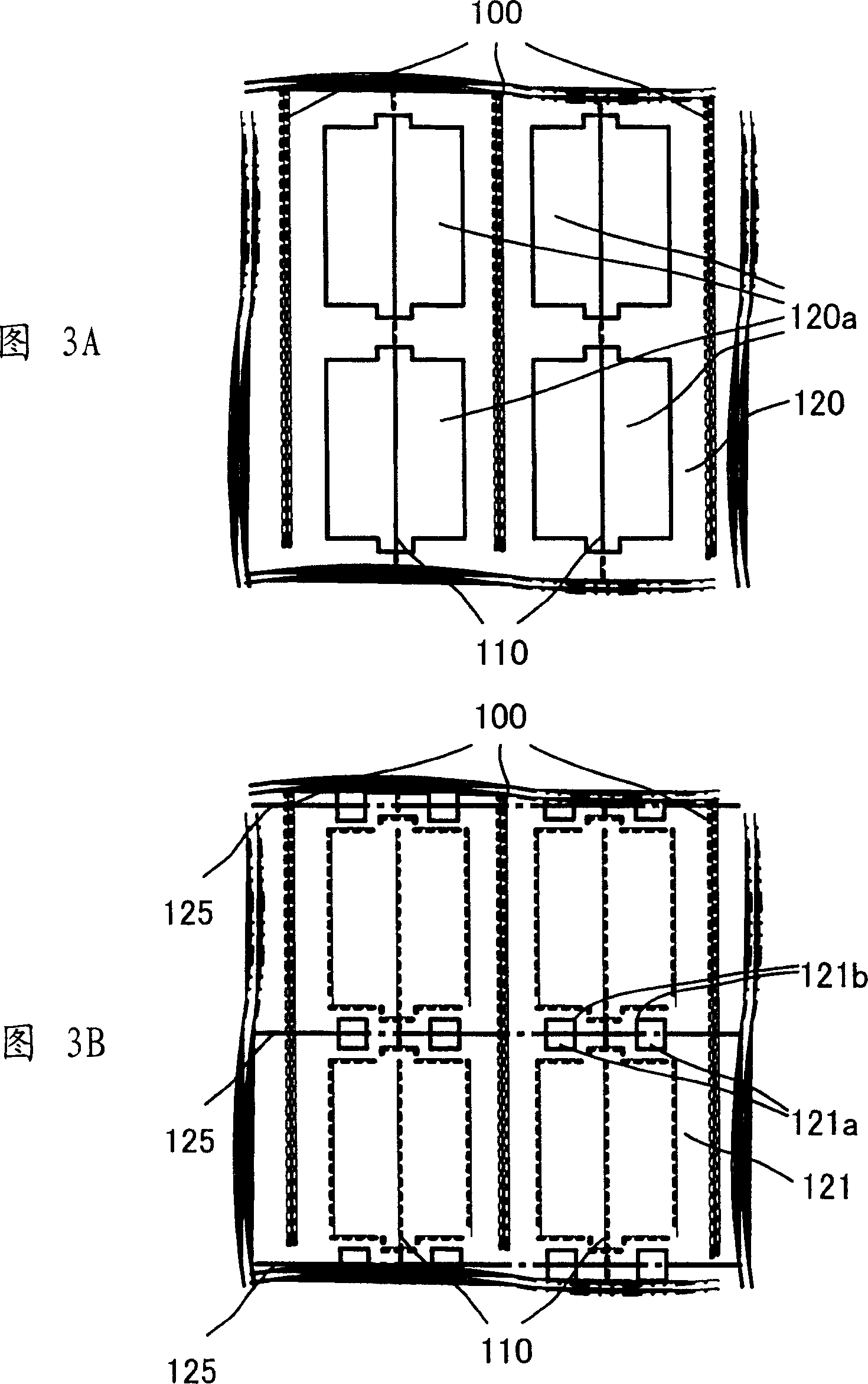
[0101] The structural outline of the nitride semiconductor laser element 10 a of this example is shown in an external perspective view shown in FIG. 6 . The structure of this nitride semiconductor laser element 10a will be described below in the manner of its manufacturing process. In the structure of the nitride semiconductor laser element 10a shown in FIG. 6, parts that can also be found in the nitride semiconductor laser element 10 shown in FIG. . Unlike Example 1, in this example, striped grooves 115a are formed in the wafer instead of grooves 115 .
[0102] In the nitride semiconductor laser element 10a of this example, the interval between the grooves 100 formed in the n-type GaN substrate 101 is 300 μm, and, on the first principal plane of the n-type GaN substrate 101, the following layer Formed sequentially: n-type GaN lower contact layer 102 with a thickness of 2.5 μm; n-type Al with a thickness of 3.0 μm 0.05 Ga 0.95 N lower cladding layer 103; by In x1 Ga 1-x1...
example 3
[0109] The structural outline of the nitride semiconductor laser element 10 b of this example is shown in an external perspective view shown in FIG. 7 . The nitride semiconductor laser element 10b is described below through its manufacturing process. In the structure of the nitride semiconductor laser element 10b shown in FIG. 7, parts of the nitride semiconductor laser element 10 shown in FIG. 5 are also found, which are designated by the same reference numerals, and explanations thereof will not be repeated. .
[0110] In the nitride semiconductor laser element 10b of this example, an n-type GaN substrate 101 in which defect-dense regions and low-defect regions are alternately arranged at intervals of 400 μm is used. First, on n-type GaN substrate 101 , grooves 100 with a width of about 5 μm are formed at an interval of about 80 μm and a depth of about 3 μm so as to be disposed on both sides of defect-intensive region 117 at an interval of about 400 μm. As a result of this...
PUM
 Abstract
Description
Claims
Application Information
 - R&D
- Intellectual Property
- Life Sciences
- Materials
- Tech Scout
- Unparalleled Data Quality
- Higher Quality Content
- 60% Fewer Hallucinations
Browse by: Latest US Patents, China's latest patents, Technical Efficacy Thesaurus, Application Domain, Technology Topic, Popular Technical Reports.
© 2025 PatSnap. All rights reserved.Legal|Privacy policy|Modern Slavery Act Transparency Statement|Sitemap|About US| Contact US: help@patsnap.com