
Conductive material for connecting part and method for manufacturing the conductive material

A technology for connecting parts and conductive materials, applied in the field of conductive materials for connecting parts, can solve the problems of reduced corrosion resistance and solderability, reduced terminal insertion force, micro-sliding wear, etc., and achieves excellent electrical reliability, friction and so on. Effect of coefficient reduction and low contact resistance

Active Publication Date: 2007-06-20
KOBE STEEL LTD
View PDF9 Cites 33 Cited by
  • Summary
  • Abstract
  • Description
  • Claims
  • Application Information

AI Technical Summary

Problems solved by technology

In addition, the insertion force of the terminal with the Cu-Sn alloy layer formed on the surface is further reduced
On the other hand, if the thickness of the Sn layer is reduced, there is a problem that the contact resistance of the terminal increases when it is kept for a long time in a high-temperature atmosphere as high as 150°C such as an engine room of a motor vehicle.
In addition, when the thickness of the Sn layer is thin, the corrosion resistance and solderability are also reduced.
In addition, the Sn layer is also prone to micro-sliding wear
In this way, in this type of terminal, the low insertion force cannot be sufficiently obtained, and after repeated plugging and unplugging, after being kept in a high-temperature atmosphere for a long time, in a corrosive environment or in a vibration environment, it can still maintain low contact resistance and other fittings. The characteristics required by the type terminal, so further improvement is required

Method used


Image

  • Conductive material for connecting part and method for manufacturing the conductive material
  • Conductive material for connecting part and method for manufacturing the conductive material
  • Conductive material for connecting part and method for manufacturing the conductive material

Examples


Embodiment 1

[0095] [Production of Cu alloy base material]

[0096] Table 1 shows the chemical components of Cu alloys (No. 1, 2) used. In this example, these Cu alloys were subjected to surface roughening treatment by mechanical means (rolling or grinding) to a Cu alloy base material having a thickness of 0.25 mm and a predetermined surface roughness. In addition, the surface roughness was measured in the following manner.

[0097] [Measurement method of surface roughness of Cu alloy base material]

[0098] It measured based on JISB0601-1994 using the contact surface roughness meter (Tokyo Seiki Co., Ltd., SURFCOM1400). The surface roughness measurement conditions were as follows: a cutoff value of 0.8 mm, a reference length of 0.8 mm, an evaluation length of 4.0 mm, a measurement speed of 0.3 mm / s, and a stylus tip radius of 5 μmR. In addition, the surface roughness measurement direction is a direction at right angles to the rolling or polishing direction performed during the surface ...

Embodiment 2

[0132] For each base material of Cu alloy No. 1 that has undergone surface roughening treatment, Cu plating with a thickness of 0.15 μm is applied, and after Sn plating with various thicknesses is performed, reflow treatment is performed at 280°C for 10 seconds. Thus, test materials (No. 11-19) were obtained. Table 4 shows the production conditions thereof. In addition, among the surface roughness parameters of the base material, the average interval Sm with respect to unevenness is all within the above-described preferable range (0.01 to 0.5 mm). In addition, the average thickness of the Cu plating and Sn plating described in Table 4 was measured in the same manner as in Example 1 above.

[0133] [Table 4]

[0134]

Test No.

base material

Ni plating

Cu plating

Sn plated

Reflow processing

Alloy

No.

arithmetic mean

Roughness: P.a

The average thickness

The average thickness

The average thickne...

Embodiment 3

[0142] For the base material of Cu alloy No. 1 with surface roughening treatment, Cu plating with a thickness of 0.15 μm was applied, and Sn plating with various thicknesses was applied, and various reflow treatments were performed to obtain test materials. (No. 20-26). Table 6 shows the production conditions thereof. In addition, among the surface roughness parameters of the base material, the average interval Sm with respect to unevenness is all within the above-described preferable range (0.01 to 0.5 mm). In addition, the average thickness of the Cu plating and Sn plating described in Table 6 was measured in the same manner as in Example 1 above.

[0143] [Table 6]

[0144]

Test No.

base material

Ni plating

Cu plating

Sn plated

Reflow processing

No.

arithmetic mean

Phase roughness: Ra

The average thickness

The average thickness

The average thickness

temperature

time

...


PUM

PropertyMeasurementUnit
Thicknessaaaaaaaaaa
The inside diameter ofaaaaaaaaaa

Abstract

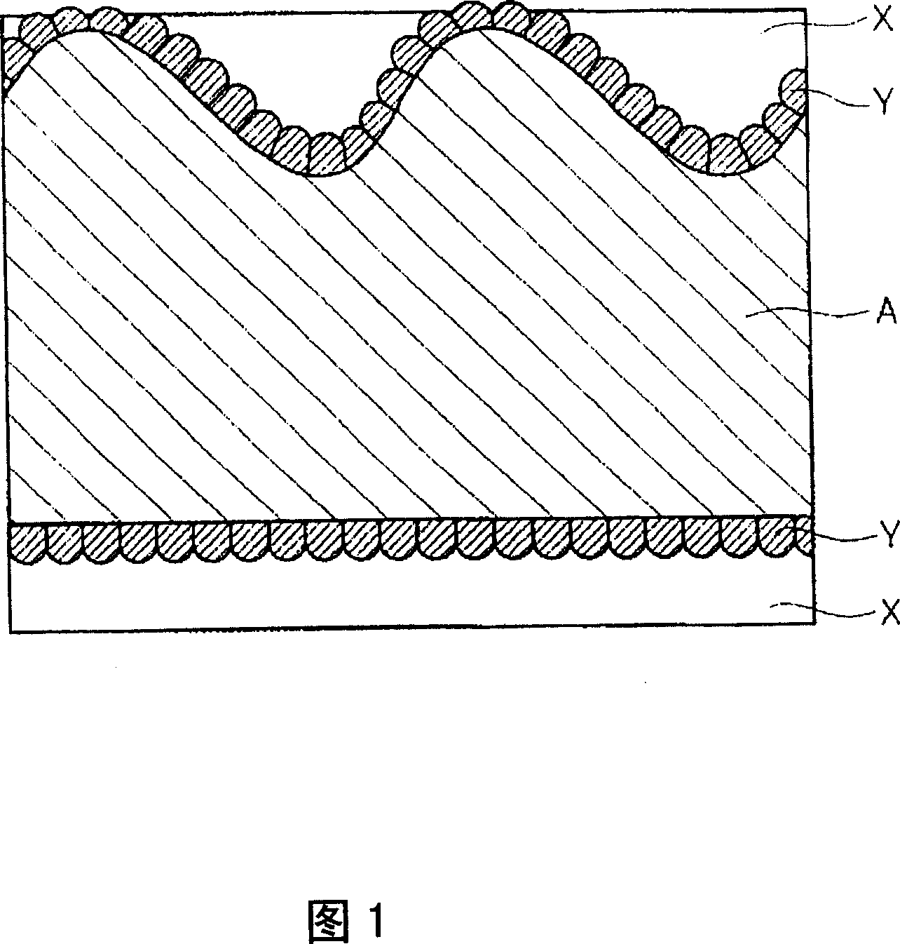
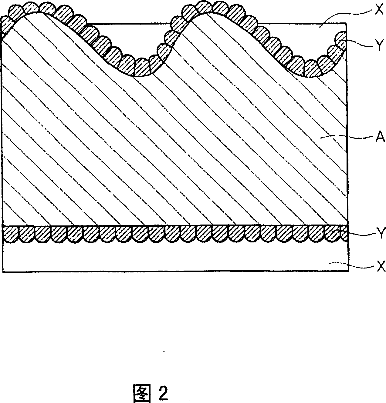
In a conductive material, on the surface of a base material composed of a Cu plate strip, a Cu-Sn alloy covering layer, which contains a Cu of 20-70at% and has an average thickness of 0.1-3.0[mu]m, and an Sn covering layer having an average thickness of 0.2-5.0[mu]m are formed in this order, and a part of the Cu-Sn alloy covering layer is exposed from the surface of the Sn covering layer at an exposing area rate of 3-75%. Reflow process is performed to the material surface, and preferably, the arithmetic average roughness Ra at least in one direction is 0.15[mu]m or more, the arithmetic average roughness Ra in all the directions is 3.0[mu]m or less, and the average thickness of the Cu-Sn alloy covering layer is 0.2[mu]m or more. The conductive material is manufactured by forming an Ni plating layer, and further, a Cu plating layer and an Sn plating layer as needed on the roughened base material surface, then by performing reflow process.

Description

technical field [0001] The present invention relates to a conductive material for connector terminals and connecting parts such as bus bars mainly used in electrical wiring of automobiles and household appliances, and particularly relates to the improvement of the friction resistance when plugging and unplugging male terminals and female terminals. It is a conductive material for fitting-type connecting parts that can reduce wear and tear, and provide electrical connection reliability during use. Background technique [0002] Among the conductive materials for connecting parts such as connector terminals and busbars used in the connection of electrical wiring of automobiles and civil equipment, in addition to requiring low-level signal voltage and current, high reliability of electrical connection is important. Except for the case of a circuit, etc., Cu or Cu alloy with Sn plating (including Sn alloy plating such as solder plating) is used. Compared with Sn plating, Au plat...

Claims


Application Information

Patent Timeline
IPC IPC(8): H01B5/02H01B13/00C25D7/00H01R13/03
Inventor 铃木基彦坂本浩杉下幸男津野理一
Owner KOBE STEEL LTD
Learn More