Packaging structure of chip with slot type metallic film supporting wire bonding

A technology of chip packaging and construction, applied in electrical components, electric solid state devices, circuits, etc., can solve problems such as inconvenience and lack of structure in products

Inactive Publication Date: 2007-07-04
WALTON ADVANCED ENG INC
View PDF0 Cites 4 Cited by
  • Summary
  • Abstract
  • Description
  • Claims
  • Application Information

AI Technical Summary

Problems solved by technology

[0005] It can be seen that the above-mentioned existing chip packaging structure obviously still has inconvenience and defects in structure and use, and needs to be further improved urgently.
In order to solve the problems existing in the packaging structure of the chip, the releva

Method used


Image

  • Packaging structure of chip with slot type metallic film supporting wire bonding
  • Packaging structure of chip with slot type metallic film supporting wire bonding
  • Packaging structure of chip with slot type metallic film supporting wire bonding

Examples


Embodiment Construction

[0070] In order to further explain the technical means and effects of the present invention to achieve the intended purpose of the invention, the following is a detailed description of the packaging structure of the slotted metal film carrying the wire-bonded chip proposed according to the present invention in conjunction with the accompanying drawings and preferred embodiments. Embodiments, structures, features and effects thereof are described in detail below.

[0071] Through the description of the specific implementation mode, when the technical means and functions adopted by the present invention to achieve the predetermined purpose can be obtained a deeper and more specific understanding, but the accompanying drawings are only for reference and description, and are not used to explain the present invention be restricted.

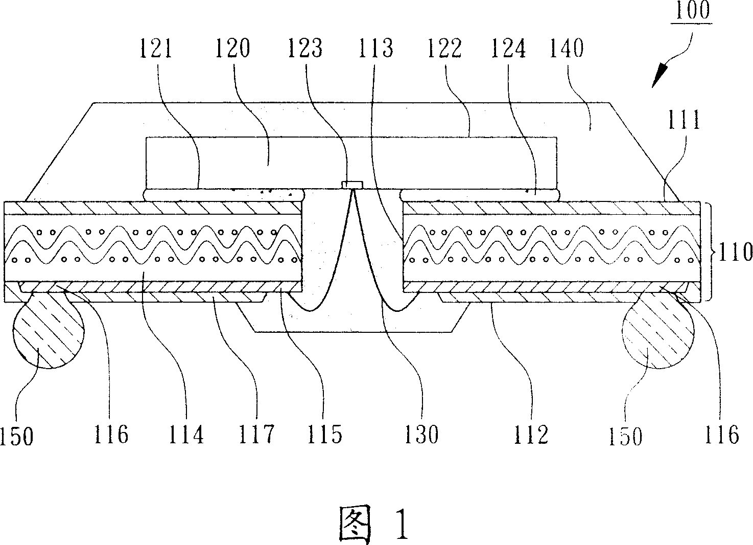
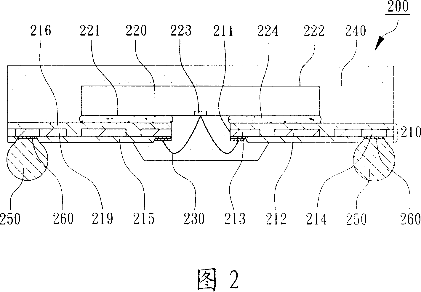
[0072] A specific embodiment of the present invention discloses a packaging structure in which a slotted metal film is used to support a wire-bonded c...


PUM

PropertyMeasurementUnit
Thicknessaaaaaaaaaa

Abstract

This invention relates to a packaging structure which using slotted metal film bearing fight line chip, and it uses a slotted metal film substrate bearing a fight line chip and chip-on-board packaging pattern, in which the slot can provide the weld wire and electrical connect the chip and the film substrate. The film substrate includes a pictorial metal core layer and at least one surface dielectric layer, and the pictorial metal core layer has the plural media and the plural external-connected pads, in which the media arranged around the slot. When the active surface of the chip attached to the film substrate, it can be very close to the pictorial metal core layer, and the pictorial metal core layer will provide good chip cooling path. Moreover, the chip package structure of the film substrate can reduce substrate costs and the thickness of the whole package, and enhance the effectiveness of thermal stress resistance.

Description

technical field [0001] The invention relates to a package structure of a chip, in particular to a chip-on-board (COB) type package structure in which a slotted metal film is used to carry a bonded chip. Background technique [0002] Chip-On-Board (COB) packaging is currently a common method in integrated circuit packaging. COB packaging mainly includes three processes: (1) the chip is directly attached to the slotted substrate, (2) the wire is electrically connected through the slot of the substrate, and (3) the chip is sealed with glue, so as to mass produce high-speed computing chips. Integrated circuit chips, especially solder balls are connected to form a ball grid array package (BGA package). It is known that the current memory chip package has developed into a COB structure to replace the previous Thin Small Outline Package (TSOP) ) and solve the dilemma that the speed cannot be increased. [0003] As shown in FIG. 1 , a conventional COB type chip packaging structure...

Claims


Application Information

Patent Timeline
IPC IPC(8): H01L23/488H01L23/31H01L23/36
CPCH01L2924/15311H01L2224/48091H01L2224/73215H01L2224/32225H01L2924/3025H01L2224/4824H01L2924/3011
Inventor 朱品华
Owner WALTON ADVANCED ENG INC
Why Eureka
Try Eureka