Objective lens system for fast scanning large FOV

a technology of objective lens and large fov, which is applied in the direction of basic electric elements, electric discharge tubes, electrical equipment, etc., can solve the problems of new and more complicated manufacturing structures, latent defects, and devices that fail electrically

Active Publication Date: 2018-06-26
ASML NETHERLANDS BV
View PDF13 Cites 3 Cited by
  • Summary
  • Abstract
  • Description
  • Claims
  • Application Information

AI Technical Summary

Problems solved by technology

The physical defects, such as foreign particles, scratch defects, residual defects, bridging defects and so on, cause the devices to fail electrically, for example, the short or open circuit.
Furthermore, since deep sub-micrometer node devices are developed, new and more complicated manufacturing structures such as a dual damascene structure and a fin-shaped field effect transistor (FinFET) structure are utilized in the semiconductor devices.
Therefore, new types of defects including latent defects, for instance, chemical mechanical polishing (CMP) scores, under-layer leakage, under-etch, missing, voids, voltage contrast (VC) defects, and non-virtual defects (NVDs) occur during the manufacturing phase.
Besides, while the less than 20 nm manufacturing process is on line, it has been a big challenge for the observation of nano-size semiconductor devices.
It is consequence that the optical inspection apparatus has been stretched to the limit of its capability at the inspection of these defects and tiny devices.
However, in terms of examination throughput, the charged particle beam apparatus remains much slower than the optical one.
However, these prior arts do not provide with the throughput improvement, and in some cases of hidden defects, for example VC defects, can't be observed by these prior arts apparatuses.
However, the very high voltage is needed to accelerate the charged particle beam resulting in the arcing problem.

Method used


Image

  • Objective lens system for fast scanning large FOV
  • Objective lens system for fast scanning large FOV
  • Objective lens system for fast scanning large FOV

Examples


Embodiment Construction

[0034]The preferred embodiment herein disclosed is not intended to be exhaustive or to limit the invention to the precise form disclosed. Rather, it is chosen and described in order to best explain the invention so that others skilled in the art may utilize its teachings. Besides, in alternative embodiments, those components identical to the components of the first embodiments are given the identical reference numerals without giving another reference numerals for simplicity.

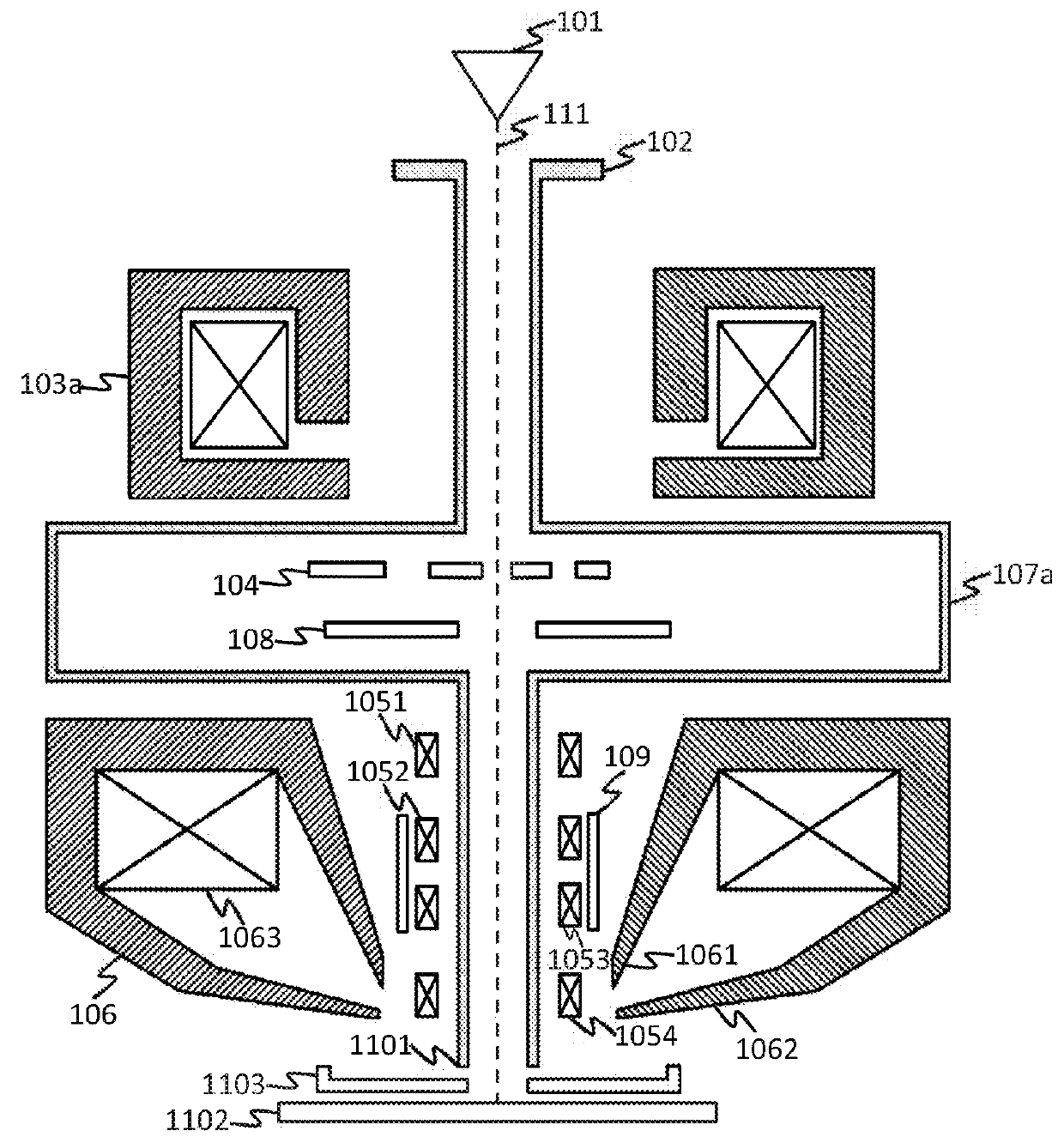
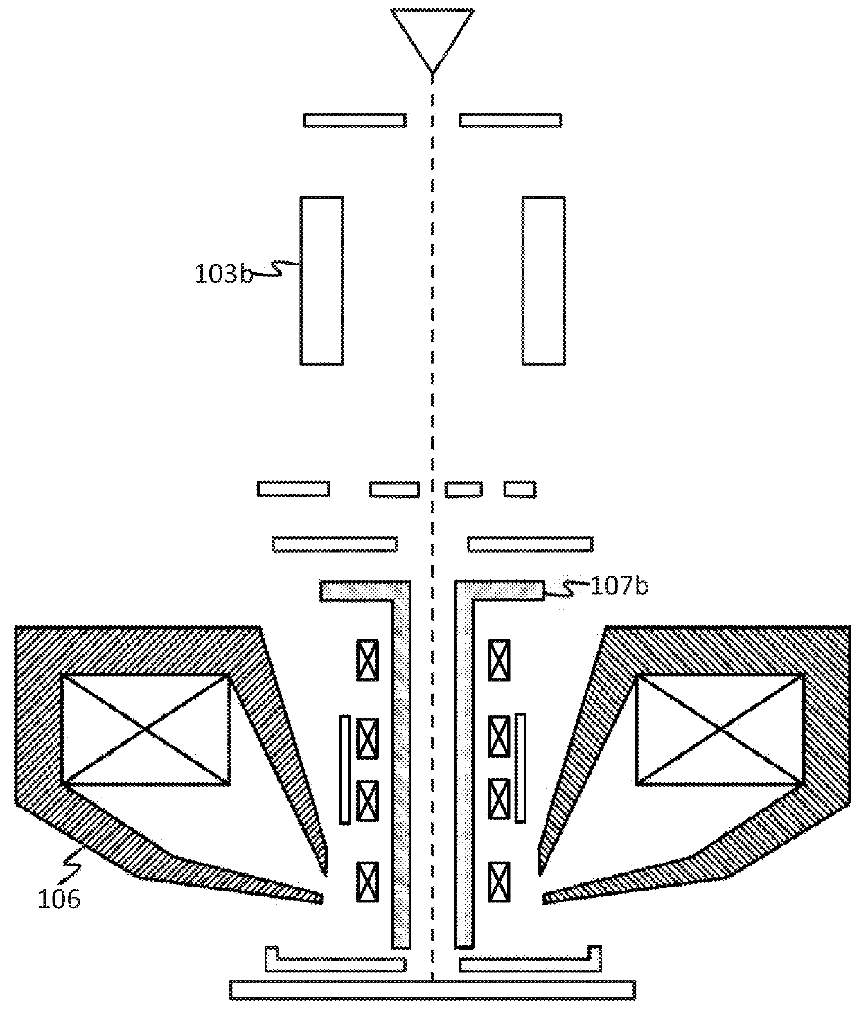
[0035]Referring now to FIG. 1a, one embodiment of a defect-inspection apparatus with a large scan field and a large beam current to inspect the defects on the wafer is described below. First, a configuration of an e-beam inspection tool, which is an axially symmetric device, according to the invention comprises inter alia main parts as an electron beam source and an electron beam column. The electron beam source typically includes an electron beam source 101 for generating a primary electron beam, an anode 102 f...


PUM


Abstract

The device includes a beam source for generating an electron beam, a beam guiding tube passed through an objective lens, an objective lens for generating a magnetic field in the vicinity of the specimen to focus the particles of the particle beam on the specimen, a control electrode having a potential for providing a retarding field to the particle beam near the specimen to reduce the energy of the particle beam when the beam collides with the specimen, a deflection system including a plurality of deflection units situated along the optical axis for deflecting the particle beam to allow scanning on the specimen with large area, at least one of the deflection units located in the retarding field of the beam, the remainder of the deflection units located within the central bore of the objective lens, and a detection unit to capture secondary electron (SE) and backscattered electrons (BSE).

Description

CLAIM OF PRIORITY[0001]This application claims all benefits accruing under 35 U.S.C. § 119 from U.S. Provisional Application No. 62 / 107,716 entitled “Objective Lens System for Fast Scanning Large FOV”, filed on the 26th day of Jan. 2015, which is incorporated by reference as if fully set forth herein.FIELD OF THE INVENTION[0002]The present invention relates to an electro-optical inspection system, and more particularly to a focusing and deflection assembly for fast scanning over a large field-of-view (LFOV) which is used in a charged particle beam column.BACKGROUND OF THE INVENTION[0003]The following description and examples are not admitted to be prior art by their mention in this Background section.[0004]In order to enhance the yield and reliability of the semiconductor devices such as integrated circuits (ICs) and memory devices, examining the defects on the patterned wafer for the avoidance of them has been significant. The physical defects, such as foreign particles, scratch de...

Claims


Application Information

Patent Timeline
Patent Type & Authority Patents(United States)
IPC IPC(8): H01J37/14H01J37/147H01J37/145H01J37/141
CPCH01J37/145H01J37/141H01J37/1477H01J37/1474H01J37/1472
Inventor LI, SHUAICHEN, ZHONGWEI
Owner ASML NETHERLANDS BV
Why Eureka
Try Eureka