Nanoantenna scanning probe tip, and fabrication methods

a scanning probe and nanoantenna technology, applied in scanning probe microscopy, measuring devices, instruments, etc., can solve the problems of preventing companies and research groups from investing in ters equipment, high variability of ters probes, and high cost and reliability of commercial tips currently on the mark

Active Publication Date: 2018-07-03
RGT UNIV OF CALIFORNIA
View PDF8 Cites 1 Cited by
  • Summary
  • Abstract
  • Description
  • Claims
  • Application Information

AI Technical Summary

Problems solved by technology

Unfortunately, typical manufacturing techniques for batch manufacturing of TERS probes yield high variability from probe tip to probe tip.
The commercial tips currently on market are expensive and unreliable.
This prevents companies and research groups from investing in TERS equipment.
There are a few examples where groups have been able to get the film to anneal into islands, creating separate nanoparticles that improve on TERS quality, they still suffer from the same problems of unpredictability, unreliability however.
Top down fabrication includes a variety of engineered TERS tips that use extremely low throughput and expensive machines (focused-ion beam and electron beam) to fabricate highly precise tips.
These tips are high performance but can take dozens of hours for highly trained individuals to fabricate.

Method used


Image

  • Nanoantenna scanning probe tip, and fabrication methods
  • Nanoantenna scanning probe tip, and fabrication methods
  • Nanoantenna scanning probe tip, and fabrication methods

Examples


Embodiment Construction

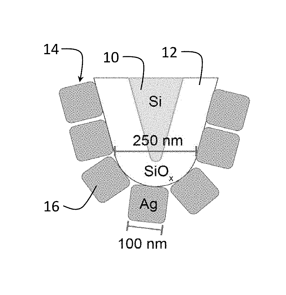
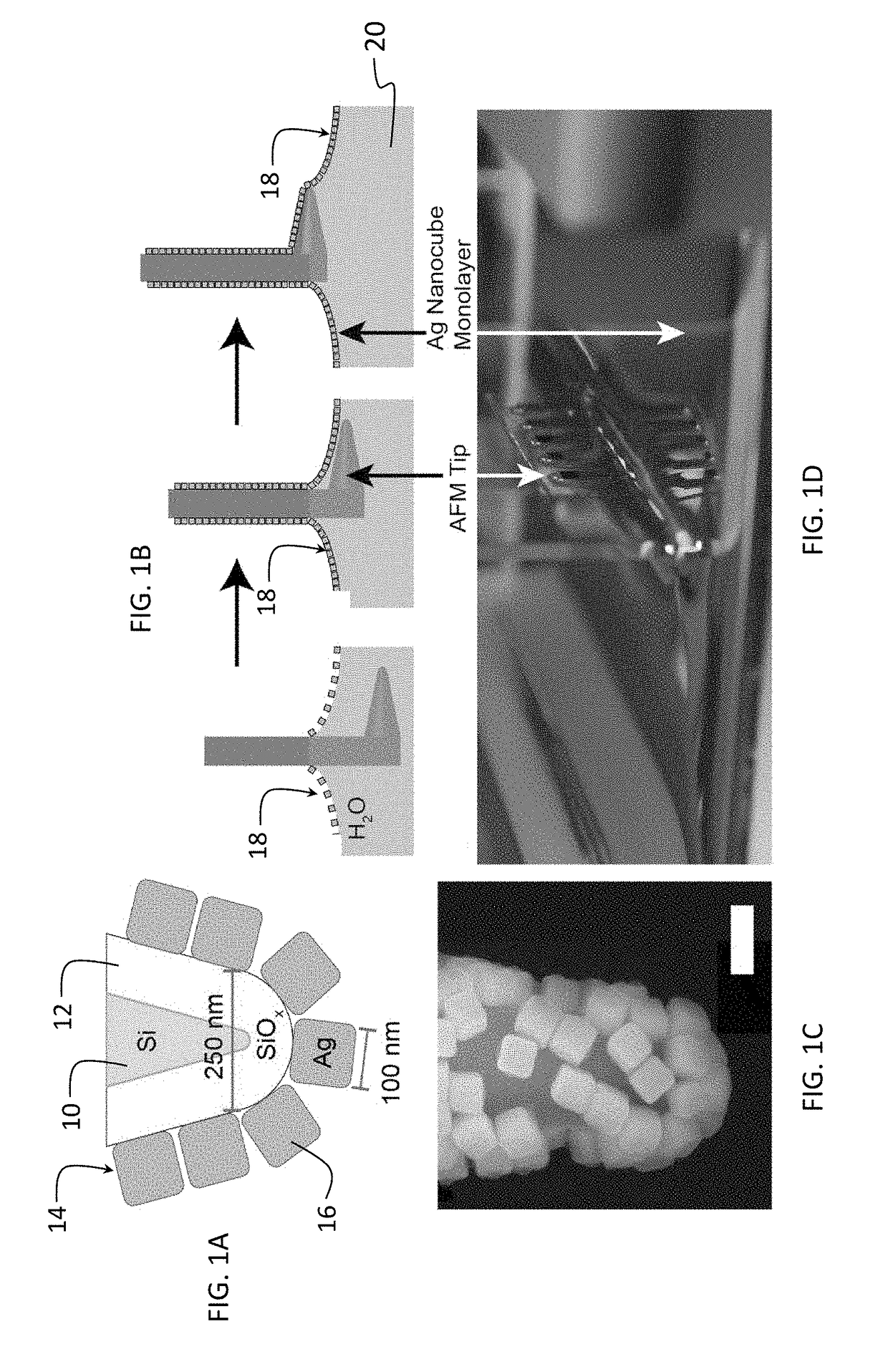
[0025]A preferred embodiment is a nanoantenna scanning probe. The scanning probe includes a sharp probe tip that is covered with contiguous film of predetermined sized and shaped plasmonic crystals. In preferred embodiments, the sharp probe tip is an AFM tip, and in other preferred embodiments the sharp probe tip is a conductive STM tip or a tuning fork tip. In preferred embodiments, the AFM tip is a blunted AFM tip. In preferred embodiments, the AFM tip is covered with a monolayer of the predetermined sized and shaped plasmonic crystals. The plasmonic crystals make the AFM probe into a nanoantenna.

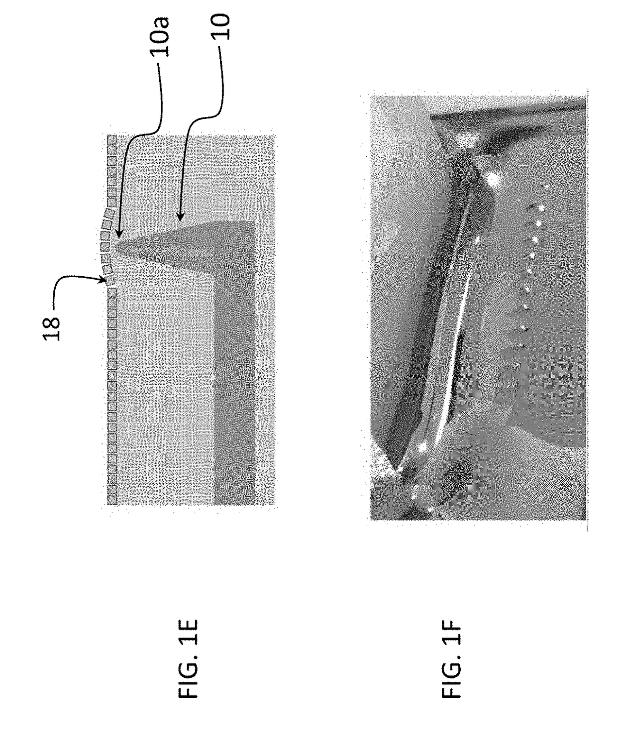
[0026]A preferred embodiment is a method for fabricating nanoantenna scanning probes. Nanoparticles having a predetermined size and shape are trapped at a liquid surface using surface tension. The nanoparticles are allowed to form a uniform and organized monolayer film. A portion of the film is transferred to sharp probe tip, such as an AFM tip, conductive STM tip or a tuning fork tip. Th...


PUM


Abstract

The invention provides a nanoantenna scanning probe tip for microscropy or spectroscopy. The nanoantenna scanning probe tip includes a sharp probe tip covered with a contiguous film of predetermined sized and shaped plasmonic nanoparticles. A method for forming the nanoantenna scanning probe tip by trapping nanoparticles having a predetermined size and shape at a liquid surface using surface tension, forming a uniform and organized monolayer film on the liquid surface, and then transferring portions of the film to a sharp probe tip. In preferred embodiments, the sharp probe tip is one of a conductive STM (scanning tunneling microscopy) tip, a tuning fork tip or an AFM (atomic force microscopy) tip. The sharp tip can be blunted with an oxide layer.

Description

PRIORITY CLAIM AND REFERENCE TO RELATED APPLICATION[0001]The application claims priority under 35 U.S.C. § 119 from prior provisional application Ser. No. 62 / 214,547, which was filed Sep. 4, 2015.STATEMENT OF GOVERNMENT INTEREST[0002]This invention was made with government support under award number D14AP00046 awarded by the Defense Advanced Research Projects Agency, award number ECCS 1125789 awarded by the National Science Foundation and under award numbers N00014-12-1-0574 and N00014-13-1-0655 awarded by the Office of Naval Research. The government has certain rights in the invention.FIELD[0003]Fields of the invention include tip-enhanced spectroscopy and atomic force microscopy, tip-enhanced Raman spectroscopy, scanning tunneling microscopy, and scanning near-field optical microscopy. Additional fields include tip-enhanced fluorescence and tip-enhanced photoluminescence. The invention is generally applicable to devices and techniques that make use of a scanning probe.BACKGROUND[0...

Claims


Application Information

Patent Timeline
Patent Type & Authority Patents(United States)
IPC IPC(8): G01Q30/02G01Q60/16G01Q60/38
CPCG01Q30/025G01Q60/38G01Q60/16G01Q30/02G01Q60/06G01Q70/14
Inventor DILL, TYLER JAMISONTAO, ANDREA RAE
Owner RGT UNIV OF CALIFORNIA
Why Eureka
Try Eureka