Nanotube tip for atomic force microscope

Inactive Publication Date: 2004-08-24
GLOBALFOUNDRIES INC
View PDF8 Cites 25 Cited by
  • Summary
  • Abstract
  • Description
  • Claims
  • Application Information

AI Technical Summary

Problems solved by technology

Despite these advantages, accurate growth of carbon nanotubes has proved to be a technical challenge.
However, the growth kinetics are not wel

Method used


Image

  • Nanotube tip for atomic force microscope
  • Nanotube tip for atomic force microscope
  • Nanotube tip for atomic force microscope

Examples


Embodiment Construction

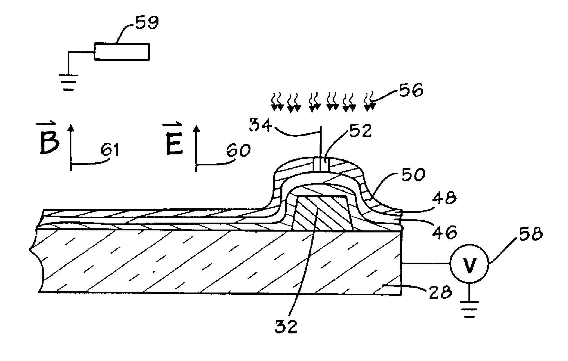
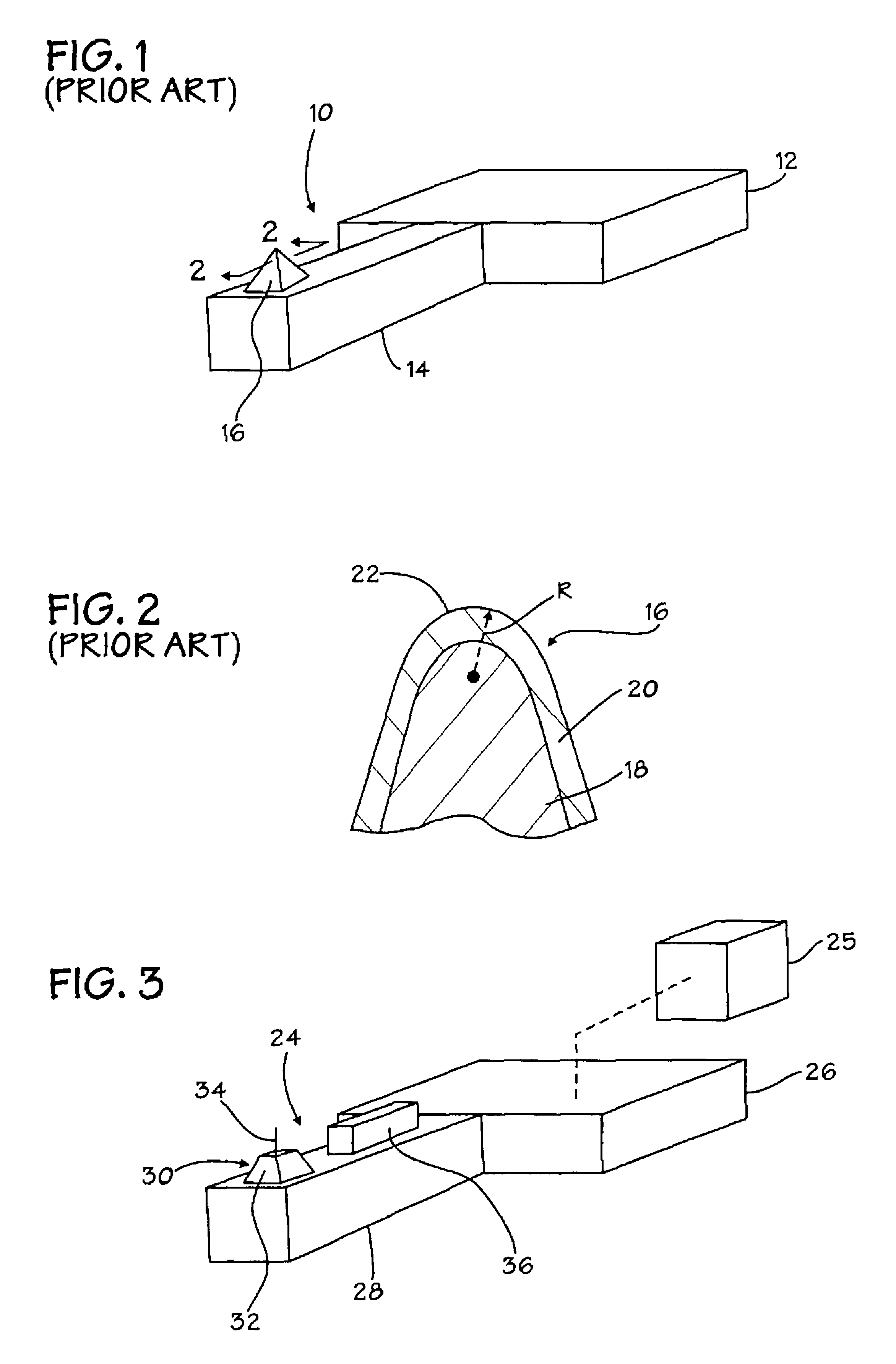
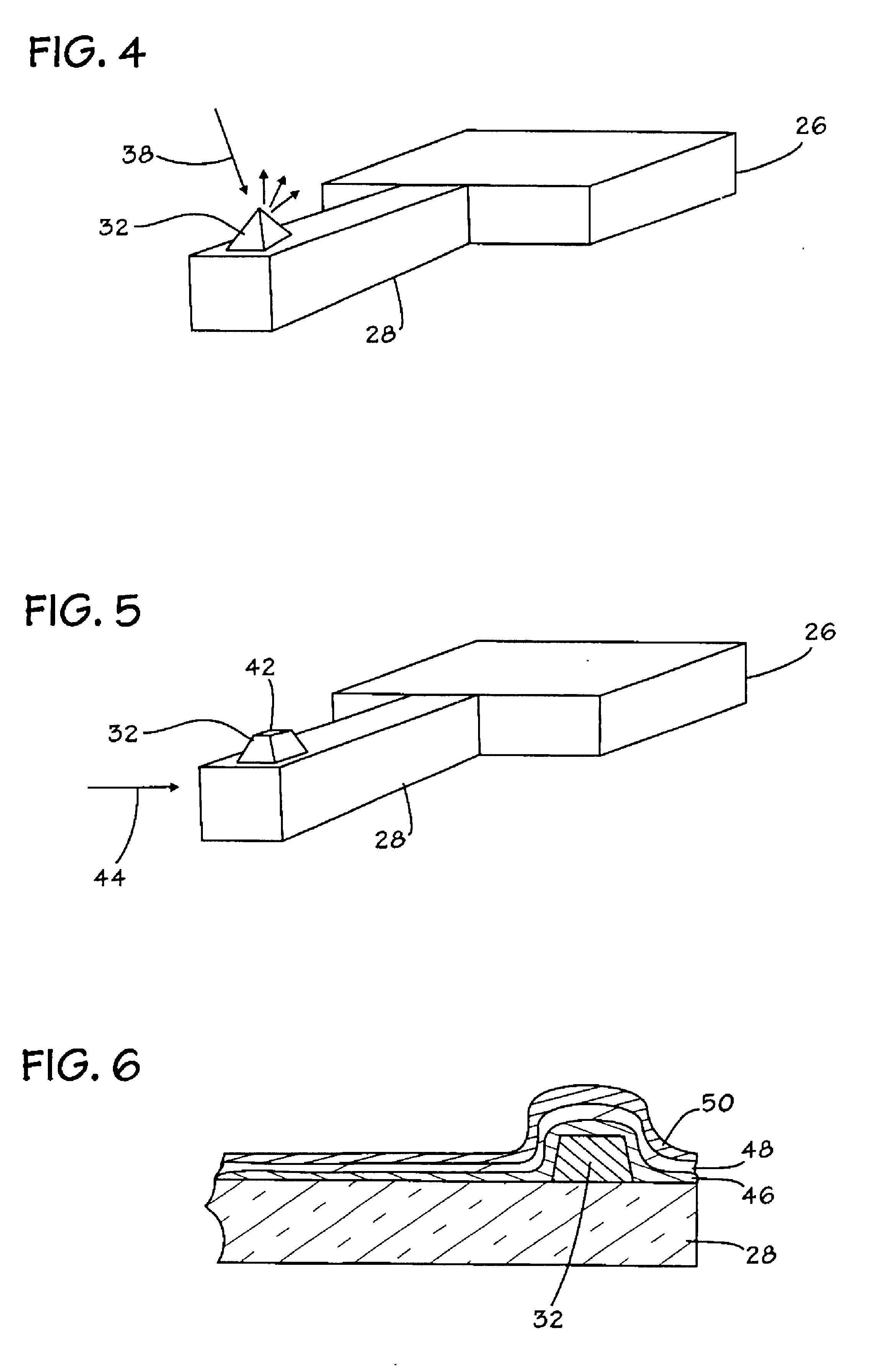
In the drawings described below, reference numerals are generally repeated where identical elements appear in more than one figure, Turning now to the drawings, and in particular to FIG. 1, therein is shown a pictorial view of a conventional atomic force microscopy ("AFM") probe 10. The probe 10 includes a base 12, a cantilever 14 and a tip 16. The cantilever 14 is frequently fabricated from silicon nitride and the base 12 is similarly fabricated from silicon nitride or another type of dielectric material. The tip 16 is commonly fabricated from silicon that has been sharpened through one or more oxidation and etching steps.

The minimum resolution provided by the tip 16 is a function of its radius of curvature. This is better seen in FIG. 2, which is a cross-sectional view of a portion of the tip 16 taken at section 2--2. The tip 16 consists of an underlying silicon structure 18 that is coated with a thin film 20 of native oxide. The minimum lateral resolution of the tip 16 is determi...


PUM


Abstract

Various microscopy probes and methods of fabricating the same are provided. In one aspect, a method of fabricating a microscopy probe is provided that includes providing a member and forming a first film on the member. The first film fosters growth of carbon nanotubes when exposed to a carbon-containing compound. A second film is formed on the first film. The second film has an opening therein that exposes a portion of the first film. A carbon nanotube is formed on the exposed portion of the first film.

Description

1. Field of the InventionThis invention relates generally to semiconductor processing, and more particularly to scanning probe tips and methods of making the same.2. Description of the Related ArtAtomic force microscopy generally involves scanning a stylus or probe across a microscopic topography, such as an integrated circuit structure, and sensing the forces exerted on the stylus. The stylus is provided with a small geometry tip that physically contacts the surface topography. The technique has been widely used in metrology of structures in photoresist, interlevel dielectric layers, sidewall angles, trench depths and surface morphology. The scanning resolution of the probe is dependent on the radius of curvature of the probe tip that contacts a given topographical feature.Early conventionally fabricated probe tips were composed of sharpened silicon. Even after multiple oxidation and etching sharpening steps, such conventional tips had a tip radius of curvature of over 10.0 nm. Tip...

Claims


Application Information

Patent Timeline
IPC IPC(8): G12B21/00G12B21/02G01Q70/12G01Q70/16
CPCB82Y15/00B82Y35/00G01Q70/12Y10S438/903Y10S977/876
Inventor GORUGANTHU, RAMA R.BRUCE, MICHAEL R.CHU, THOMASSANTANA, JR., MIGUELPOWELL, ROBERT
Owner GLOBALFOUNDRIES INC
Why Eureka
Try Eureka