Probe tip and method of manufacturing tips and probes for detecting microcurrent or microforce

a technology of microcurrent or microforce, which is applied in scanning probe microscopy, decorative arts, nanotechnology, etc., can solve the problems of substrate not being re-used, metal coating rapidly wears off, time-consuming steps, etc., and achieves cost-effective and time-saving effects, avoiding backside lithography and time-consuming etching steps

Inactive Publication Date: 2002-04-25
INTERUNIVERSITAIR MICRO ELECTRONICS CENT (IMEC VZW)
View PDF0 Cites 25 Cited by
  • Summary
  • Abstract
  • Description
  • Claims
  • Application Information

AI Technical Summary

Benefits of technology

[0019] It is an aim of the invention to achieve a cost and time efficient method to manufacture probes used in scanning microscopy, e.g. AFM, STM, SSRM or likewise. This method comprises front side processing steps and avoids the backside lithography and time consuming etching steps required to create a probe membrane or to release the probe membrane. This method requires one substrate to form a full probe consisting of a probe tip, cantilever and probe membrane. This method allows easy removal of the probe prior to mounting the probe into a scanning microscope.
[0021] It is one object of the invention to disclose a cost and time efficient method to manufacture probes used in scanning microscopy, e.g. AFM, STM, SSRM or likewise. This method comprises front side processing steps and avoids the backside lithography and time consuming etching steps required to create a probe membrane or to release the probe membrane.

Problems solved by technology

Silicon (Si) tips with a thin metal coating, typically 10-25 nm thick, are commercially available since the early 1990's but the metal coatings rapidly wear off.
1. The wafer needs to be processed from both sides whereby precautions have to be taken to protect the non-processed side.
2. A lithographic tool, e.g. a mask aligner, is required to align patterns defined on the backside of the substrate to the front or topside of the wafer.
3. The backside of the silicon substrate will be etched to release at the front-side the cantilever with metal tip (see FIG. 1a,e) and hence the substrate cannot be re-used.
4. This backside etching requires wafer scale uniformity of e.g. wafer thickness, etch speed, etch selectivity to avoid local over-etching of the tip and / or probe and it is a time consuming step.
5. During this etch step the tip, e.g. its radius or sidewalls, can be modified by the etch chemicals.
1. Two substrates are required to manufacture a probe tip with cantilever.
2. The metal, peeling layer and substrate have to be chosen such to obtain the correct relative strength of the different layers to allow tearing off the first second substrate from the probe tip.
3. The second substrate still requires an etching of the rear surface to define a cantilever and to release the probe tip. All problems related to such rear side etching remains.

Method used


Image

  • Probe tip and method of manufacturing tips and probes for detecting microcurrent or microforce
  • Probe tip and method of manufacturing tips and probes for detecting microcurrent or microforce
  • Probe tip and method of manufacturing tips and probes for detecting microcurrent or microforce

Examples


first embodiment

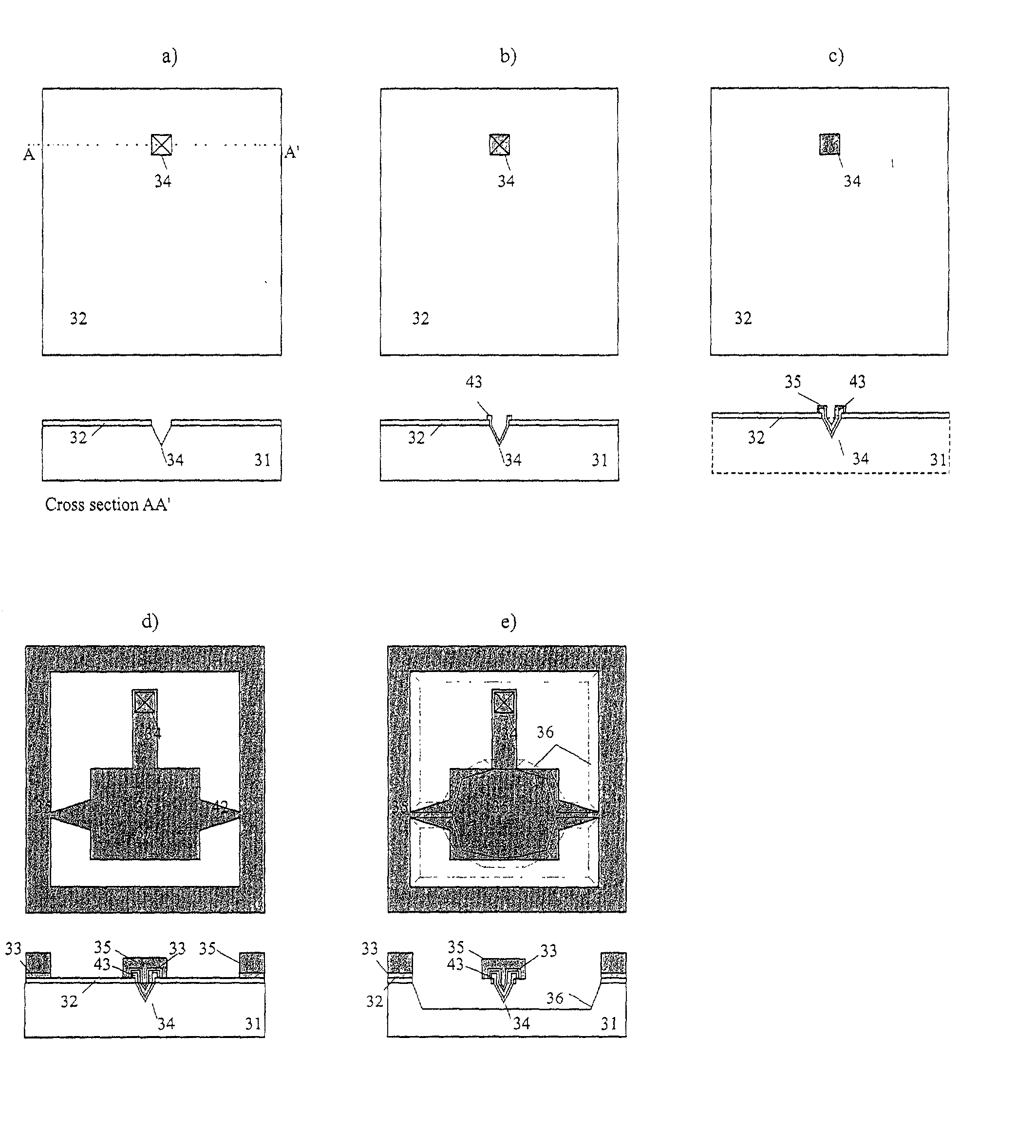
[0042] In a first embodiment, a method of manufacturing a scanning probe requiring only front side processing steps is disclosed. This method comprises two front side lithographic steps. The peel-off effect is achieved by selectively metallising the area of the probe tip configuration. This metal layer has a sufficiently high enough adhesion to the substrate to allow further processing, but this adhesion force is weak enough to be overcome when peeling the probe gradually from the wafer.

[0043] This method comprises the following steps. During the first patterning step a mould (34a) is formed in the starting substrate (31), preferably a silicon wafer. (FIG. 3a) This mould may have one of various shapes, e.g., pyramidal, a truncated cone, a cylinder. In case a silicon wafer is used a truncated pyramidal etch pit is formed by anisotropically etching the substrate trough an opening defined in a masking layer formed on top of the substrate. Such a masking layer can be a photo resist or a...

second embodiment

[0048] In a second embodiment, the method of manufacturing a full metal probe with two front side lithographic steps is disclosed.

[0049] The starting substrates (31) were (100)-Si wafers having a diameter of 150 mm. These wafers were covered with 470 nanometer (nm) thermally grown oxide (32), SiO.sub.2, and 150 nm low-pressure chemical vapour deposited (LPCVD) nitride, Si.sub.3N.sub.4. (see FIG. 3a) Photoresist was spun onto the wafers and squares (34) of 40.times.40 square micrometer (.mu.m.sup.2) were opened in the photoresist during the first lithography step. These squares define the tip area (34). This resist pattern was then transferred to the Si.sub.3N.sub.4 layer by reactive ion etching (RIE) using a SF.sub.6:O.sub.2 etching mixture. Next, the resist was removed and the nitride pattern was transferred to the SiO.sub.2 layer by etching the oxide layer with buffered HF (BHF). Inverted pyramids were then etched in 30% KOH at 70.degree. C. for 55 minutes. The wafer surface was c...


PUM

PropertyMeasurementUnit
thickaaaaaaaaaa
diameteraaaaaaaaaa
thickaaaaaaaaaa

Abstract

A full metal probe and a method of making the metal probe for electrical atomic force microscopy. In one embodiment, the method comprises manufacturing the full metal probe using two lithography steps. The step of etching thin membranes is dropped or eliminated to substantially reduce the processing time. Thus, topside processing is sufficient. The probe and tip can be peeled off from the wafer using a metallization procedure.

Description

RELATED APPLICATIONS[0001] This application claims priority under 35 U.S.C. .sctn. 119 to U.S. provisional application entitled "METHOD FOR MANUFACTURING TIPS AND PROBES FOR DETECTING MICROCURRENT OR MICROFORCE AND DEVICES OBTAINED THEREOF", having Application No. 60 / 233,276, and filed on Sep. 18, 2000. This application also claims priority under 35 U.S.C. .sctn. 119 to European patent application number EP 00870246.6, filed on Oct. 27, 2000.BACKGROUND OF THE INVENTION[0002] 1. Field of the invention[0003] The invention is generally related to a scanning tunnelling or atomic force microscope and more particularly to the manufacturing of tip and probe used in said scanning tunnelling or atomic force microscope.[0004] 2. Description of the Related Art[0005] Scanning tunnelling microscopy (STM) and electrical atomic force microscopy (AFM) enables us today to carry out electrical and / or topographical measurements on modern semiconductor devices with nanometer (nm) spatial resolution. Th...

Claims


Application Information

Patent Timeline
Patent Type & Authority Applications(United States)
IPC IPC(8): G01Q60/10G01Q60/16G01Q60/24G01Q60/38G01Q70/14G01Q70/16
CPCB82Y35/00Y10S977/875G01Q70/16G01Q70/06
Inventor HANTSCHEL, THOMASVANDERVORST, WILFRIED
Owner INTERUNIVERSITAIR MICRO ELECTRONICS CENT (IMEC VZW)
Why Eureka
Try Eureka