Stress induction in 3D device channel using elastic relaxation of high stress material

a stress induction and high stress technology, applied in the field ofsemiconductor devices, can solve the problems of large challenges for the use of traditional external stressors in channel materials, no clear equivalent solution for compressive stress, and the failure of sige layers to be very defectiv

Active Publication Date: 2018-07-10
IBM CORP
View PDF15 Cites 9 Cited by
  • Summary
  • Abstract
  • Description
  • Claims
  • Application Information

AI Technical Summary

Problems solved by technology

As the device density increases, greater challenges for use of traditional external stressors in channel materials exist.
A relaxed SiGe buffer can be used to induce tensile stress in silicon but no clear equivalent s

Method used


Image

  • Stress induction in 3D device channel using elastic relaxation of high stress material
  • Stress induction in 3D device channel using elastic relaxation of high stress material
  • Stress induction in 3D device channel using elastic relaxation of high stress material

Examples


Embodiment Construction

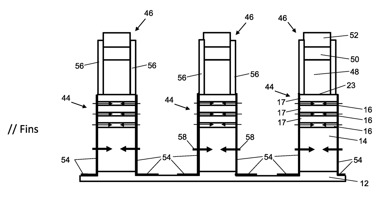
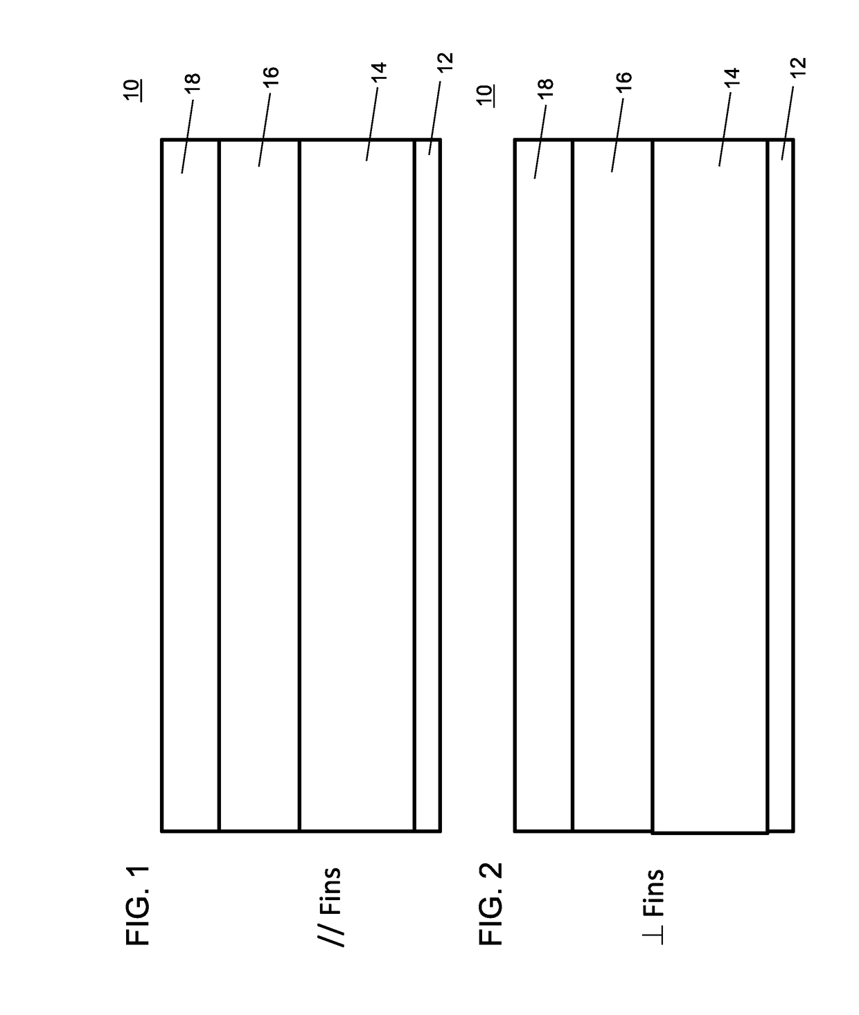
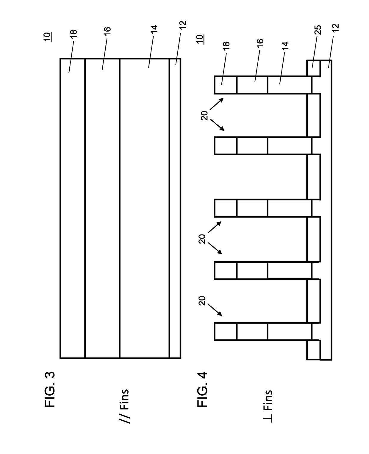
[0036]In accordance with aspects of the present invention, methods and structures are provided to form compressively strained structures. In some embodiments, one or more semiconductor layers or fin structures are rendered compressive. In one example, compressive properties can be applied to a semiconductor layer when a compound is inserted into a lattice of the semiconductor material to alter a lattice constant of the semiconductor material. The compound can include a material that is a crystalline compound and is preferably chemically bound with the material of the lattice. The compound can thus form a semiconductor crystal within a semiconductor matrix and affect the lattice constant of the overall layer.

[0037]In one embodiment, a tensily strained layer can be formed on a substrate to induce tension in an adjacent layer (e.g., device channel). The tensily strained layer may include Si3P4 on Si or SiC on Si, although other material combinations may be employed. The tensily straine...


PUM


Abstract

A method for inducing stress in a device channel includes forming a stress adjustment layer on a substrate, the stress adjustment layer including an as deposited stress due to crystal lattice differences with the substrate. A device channel layer is formed on the stress adjustment layer. Cuts are etched through the device channel layer and the stress adjustment layer to release the stress adjustment layer to induce stress in the device channel layer. Source/drain regions are formed adjacent to the device channel layer.

Description

BACKGROUNDTechnical Field[0001]The present invention generally relates to semiconductor devices, and more particularly to substrates and methods for fabrication that yield a compressive strain employed for formation of semiconductor devices.Description of the Related Art[0002]As the device density increases, greater challenges for use of traditional external stressors in channel materials exist. A relaxed SiGe buffer can be used to induce tensile stress in silicon but no clear equivalent solution for compressive stress exists. SiGe layers can be very defective if above a critical thickness, implanted or subjected to a high thermal budget.[0003]Strained silicon and strained silicon-on-insulator (SOI) can provide enhanced properties for semiconductor devices. For example, p-type field effect transistors (PFETs) have improved performance when formed with a compressive strain channel, and n-type field effect transistors (NFETs) have improved performance when formed with a tensile strain...

Claims


Application Information

Patent Timeline
IPC IPC(8): H01L27/088H01L29/06H01L21/306H01L29/66H01L29/78
CPCH01L29/7849H01L29/785H01L29/7848H01L29/0665H01L21/30604H01L29/66795B82Y10/00H01L29/0673H01L29/0847H01L29/1054H01L29/66439H01L29/775
Inventor CHENG, KANGGUOLOUBET, NICOLAS J.MIAO, XINREZNICEK, ALEXANDER
Owner IBM CORP
Why Eureka
Try Eureka