Mosfet having a high stress in the channel region

a channel region and high stress technology, applied in the field of high-performance semiconductor devices, can solve the problems of linear proportionality of the amount of lateral recesses, difficult to adapt to soi devices, and difficulty in recessed regions, so as to improve the uniformity of etching, minimize loading effects, and improve control

Inactive Publication Date: 2009-07-09
GLOBALFOUNDRIES INC
View PDF4 Cites 57 Cited by
  • Summary
  • Abstract
  • Description
  • Claims
  • Application Information

AI Technical Summary

Benefits of technology

[0012]An advantage of the present invention is that etch process is self-aligning to the edges of the source and drain extension regions so that the etch profile is better controlled and is independent of pattern density of the etched regions, i.e., loading effects are minimized resulting in improved uniformity of etch relative to prior art etch processes.
[0013]Further, an abrupt junction profile may be obtained since the sharpness of the boundaries between the source and drain extension regions is not limited by thermal diffusion but may be formed by an abrupt interface introduced by in-situ doped epitaxy. Alternatively, the dopants may be introduced into the source and drain regions and the deep source and drain regions by an intrinsic epitaxial deposition followed by a dopant implantation and an anneal. The embedded stress-generating material may provide additional advantages of suppressing dopant diffusion resulting in an abrupt dopant profile in source and drain extension regions and / or deep source and drain regions containing some stress-generating alloys. For example, boron diffusion is reduced significantly in SiGeC alloys and phosphorus diffusion is suppressed in Si:C alloys. The abrupt junction profile reduces short-channel effects and series resistance in the source and drain extension regions and / or the deep source and drain regions.
[0014]Yet another advantage of the present invention is that heterojunctions (junctions between two heterogeneous semiconductor materials) between the semiconductor material comprising a body of a MOSFET and the embedded stress-generating materials are in close proximity to the p-n junctions (metallurgical junctions formed at the boundary between two semiconductor regions having opposite dopant types). It has been shown that the junction leakage remains low and a hetero-barrier can help reduce drain induced barrier lowering (DIBL) and an off-current as long as the heterojunction is contained in close proximity of the p-n junction.
[0015]According to an aspect of the present invention, a semiconductor structure is provided, which comprises:
[0016]a semiconductor substrate containing a first semiconductor material and including a body having a doping of a first conductivity type, wherein the body abuts a top surface of the semiconductor substrate;
[0017]a gate electrode including a gate dielectric and a gate conductor, wherein the gate dielectric vertically abuts the body;

Problems solved by technology

However, forming such an etch profile in the recessed region poses a challenge in processing.
One typical problem is that the amount of lateral recess is linearly proportional to the vertical etch depth during an isotropic etch, for either a dry etch or a wet etch.
While this technique may be used for silicon recess in bulk devices which have relatively deep source and drain regions, it is not suitable for SOI devices.
Another typical problem of currently known etching techniques is a loading effect, in which the etch profile depends on pattern density, i.e., a local areal density of etchable materials.
A third typical problem is that the etch profile of an isotropic or anisotropic recess etch may contain crystallographic facets formed on the surfaces of the recessed regions, which poses a challenge for a subsequent epitaxial growth of embedded materials.
Further, such a reactive ion etch process may potentially have a very small process window.

Method used


Image

  • Mosfet having a high stress in the channel region
  • Mosfet having a high stress in the channel region
  • Mosfet having a high stress in the channel region

Examples


first embodiment

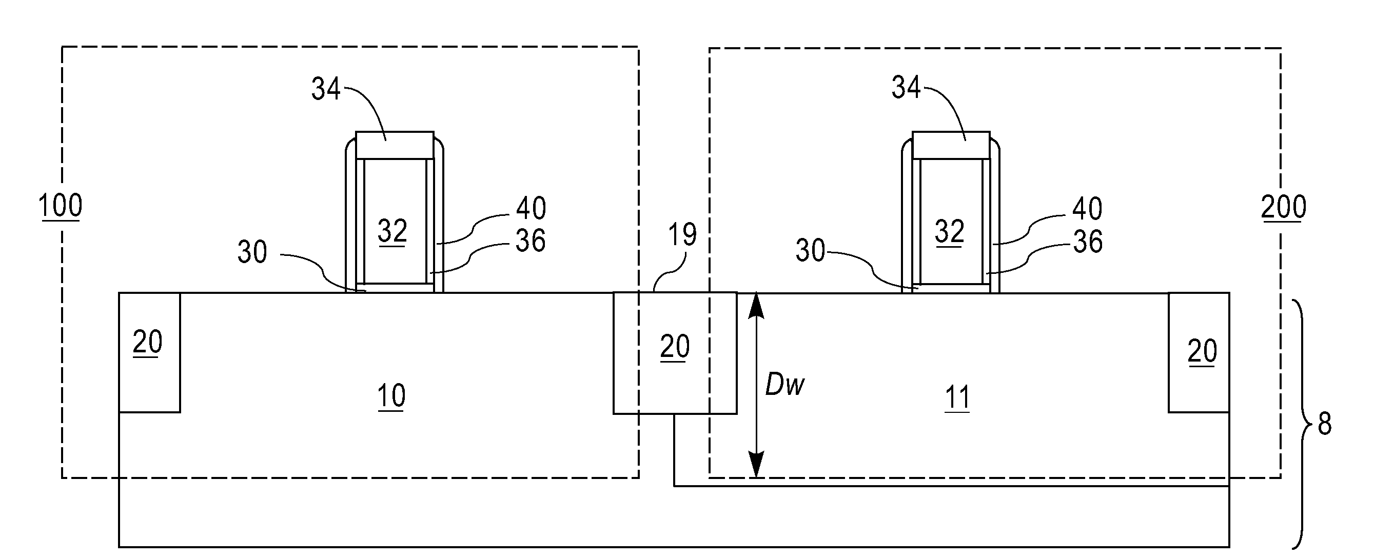
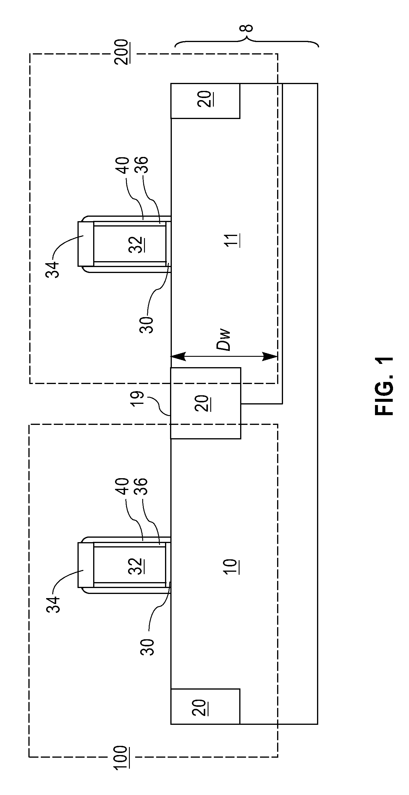
[0076]Referring to FIG. 1, a first exemplary semiconductor structure according to the present invention is shown, which comprises a semiconductor substrate 8 containing a first semiconductor region 10 and shallow trench isolation 20. The first semiconductor region 10 comprises a first semiconductor material having a doping of a first conductivity type at a first dopant concentration. The semiconductor substrate 8 may further contain a second semiconductor region 11 comprising the first semiconductor material and having a doping of a second conductivity type, wherein the second conductivity type is the opposite of the first conductivity type. The first semiconductor region 10 may have a p-type doping and the second semiconductor region 11 may have an n-type doping, or vice versa. Typically, the second semiconductor region 11 comprises a well extending from a top surface 19 of the semiconductor substrate to a well depth Dw into the semiconductor substrate 8.

[0077]The first semiconduct...

second embodiment

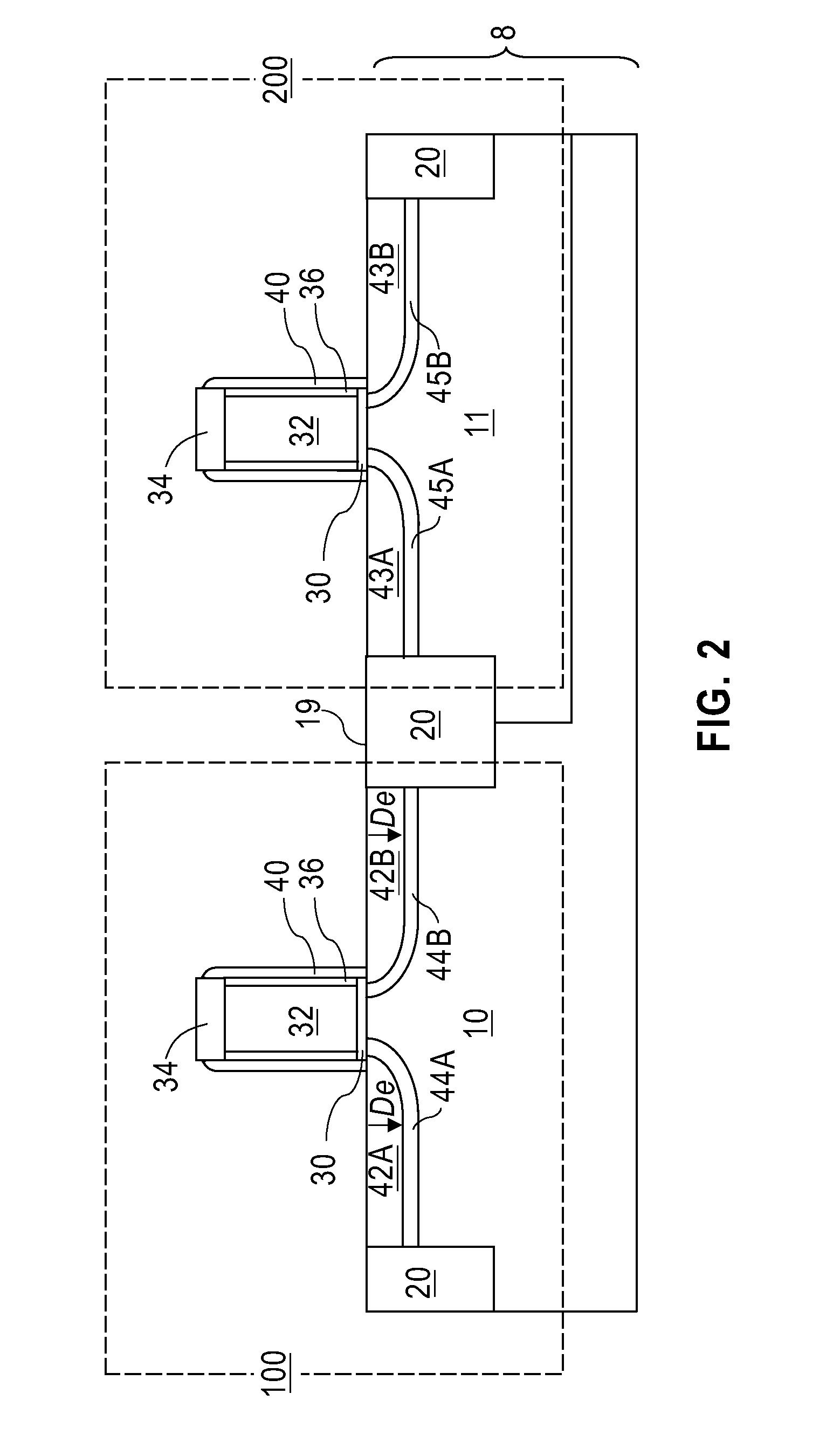
[0108]Referring to FIG. 10, a second exemplary semiconductor structure according to the present invention is derived from the first exemplary structure in FIG. 1. A dummy first source extension region 12A, a dummy first drain extension region 12B, a second source extension region 43A, and a second drain extension region are formed in the semiconductor substrate 8 by ion implantation of dopants of the first conductivity type. Thus, the first semiconductor region 10, the dummy first source extension region 12A, and the dummy first drain extension region 12B have the first conductivity type doping. The dopant concentration of the dummy first source extension region 12A and the dummy first drain extension region 12B is substantially higher than the first dopant concentration. The dopant concentration of the dummy first source extension region 12A and the dummy second drain extension region 12B may be from about 3.0×10¹⁸ / cm3 to about 3.0×10²¹ / cm3, and typically from about 3.0×10¹⁹ / cm3 to...


PUM

PropertyMeasurementUnit
lattice constantsaaaaaaaaaa
thicknessaaaaaaaaaa

Abstract

Source and drain extension regions are selectively removed by a dopant concentration dependent etch or a doping type dependent etch, and an embedded stress-generating material such as SiGe alloy or a Si:C alloy in the source and drain extension regions is grown on a semiconductor substrate. The embedded stress-generating material may be grown only in the source and drain extension regions, or in the source and drain extension regions and in deep source and drain regions. In one embodiment, an etch process that removes doped semiconductor regions of one conductivity type selective to doped semiconductor regions of another conductivity type may be employed. In another embodiment, a dopant concentration dependent etch process that removes doped semiconductor regions irrespective of the conductivity type selective to undoped semiconductor regions may be employed.

Description

FIELD OF THE INVENTION[0001]The present invention relates to high-performance semiconductor devices for digital or analog applications, and more particularly to complementary metal oxide semiconductor (CMOS) devices that have stress induced mobility enhancement. Specifically, the present invention provides stressed CMOS devices with embedded stress-inducing material in the source and drain extension regions that laterally protrude from deep source and drain regions toward a channel so that heterojunctions between two semiconductor materials coincide with, or are located in close proximity to, p-n junctions, and methods of manufacturing the same.BACKGROUND OF THE INVENTION[0002]Various techniques for enhancing semiconductor device performance through manipulation of carrier mobility have been investigated in the semiconductor industry. One of the key elements in this class of technology is the manipulation of stress in the channel of transistor devices. Some of these methods utilize ...

Claims


Application Information

Patent Timeline
Patent Type & Authority Applications(United States)
IPC IPC(8): H01L21/8238H01L27/092
CPCH01L21/823807H01L21/823814H01L29/165H01L29/6653H01L29/66537H01L29/7848H01L29/6656H01L29/6659H01L29/66636H01L29/7833H01L29/66545
Inventor OUYANG, QIQINGSCHONENBERG, KATHRYN T.YATES, III, JOHN
Owner GLOBALFOUNDRIES INC
Why Eureka
Try Eureka