
Single-mode polymer waveguide connector assembly

a single-mode, polymer technology, applied in the direction of instruments, film/foil adhesives, optical elements, etc., can solve the problem of reducing the latency of optical communication over large distances

Inactive Publication Date: 2018-10-23
IBM CORP
View PDF14 Cites 12 Cited by
  • Summary
  • Abstract
  • Description
  • Claims
  • Application Information

AI Technical Summary

Benefits of technology

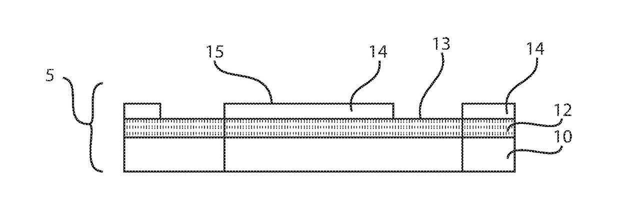
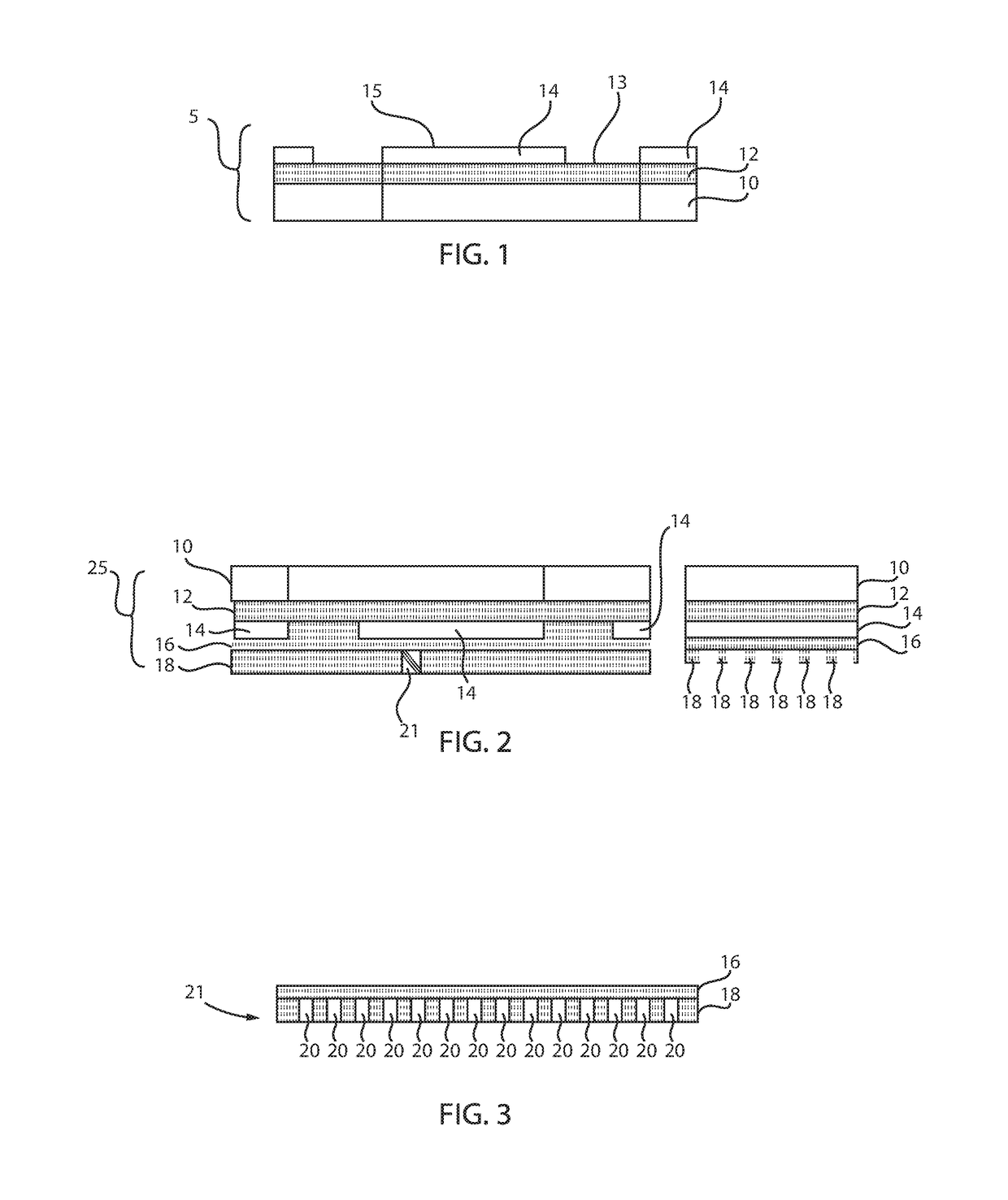
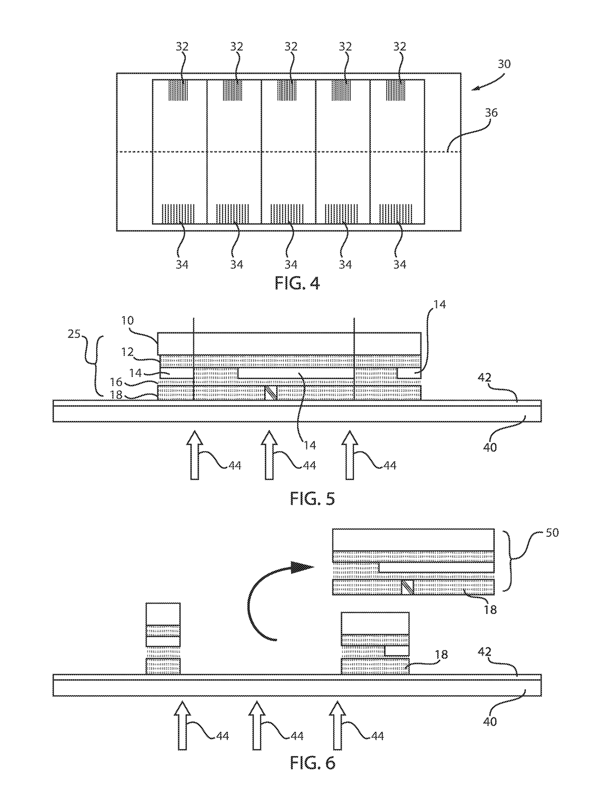
This patent describes a method for making polymer waveguide chips for use in silicon photonic packaging. The method involves preparing a polymer waveguide sheet with partially exposed cores and cladding, and then using a dicing tape to separate the layers. A method is also provided for aligning a polymer waveguide array with a silicon waveguide array on a silicon chip, creating an adiabatic coupling. The technical effect of this patent is to provide a reliable and efficient method for fabricating polymer waveguide chips for silicon photonic packaging.

Problems solved by technology

In addition, since information propagates through optical fibers at the speed of light, latency is decreased over large distances using optical communications.

Method used


Image

  • Single-mode polymer waveguide connector assembly
  • Single-mode polymer waveguide connector assembly
  • Single-mode polymer waveguide connector assembly

Examples


Embodiment Construction

[0024]Embodiments in accordance with the present invention provide methods and devices for cleaning a surface of a polymer waveguide (PWG) core array at a silicon side of a PWG chip in order to realize highly efficient adiabatic coupling. Both multimode and single-mode polymer waveguides (PWG) are widely used either in a rigid form on a printed board, or in a flexible form on a polymer base film. The principle of an optical waveguide (WG) is that a combination of core and clad (or cladding), which is a combination of two different type polymers having a different refractive index, is provided and the core is used as a light transmitting path. On the other hand, silicon waveguides (SiWG) in which a light transmitting path is fabricated on a silicon (Si) chip are also widely used. Both in the PWG and in the SiWG, multi-channel waveguides are fabricated in an array in one direction in parallel with each other so that multi-channel light transmitting paths are provided.

[0025]Embodiments...


PUM


Abstract

A method of fabricating a polymer waveguide (PWG) is presented. The method includes preparing a polymer waveguide (PWG) sheet having a surface with partially exposed cores and partially exposed cladding, the cladding covering the cores and preparing a first dicing tape, the first dicing tape being an ultraviolet (UV) cut type dicing tape defining separation lines on a back side thereof. The method further includes placing the partially exposed cores of the PWG sheet on the first dicing tape to prevent the surface of the PWG sheet from atmospheric contaminations and placing a tape side of the first dicing tape attached to the PWG sheet on a second dicing tape.

Description

BACKGROUNDTechnical Field[0001]The present invention relates generally to optical waveguides, and more specifically, to a single-mode polymer waveguide connector.Description of the Related Art[0002]Waveguides are used to transport optical signals over large distances with very low losses. Waveguides employ a difference between a refractive index for an internal medium called “core” and an external medium called “clad.” In fiber optics, the transport medium “core” is made of a higher refractive index glass and the external medium “clad” is made of a lower refractive index glass. These two glass layers are surrounded by sheath, shielding, or air. When an optical signal in the inner core layer hits a boundary between core and clad, it is internally reflected instead of escaping from the core layer. Thus, optical fibers can be used to transport very low-loss signals across long distances.[0003]Optical fibers used for waveguides are thin, flexible, and frequently made of silica glass. Ap...

Claims


Application Information

Patent Timeline
IPC IPC(8): G02B6/30G02B6/122G02B6/12
CPCG02B6/30G02B6/122C09J7/02G02B2006/12035C09J2203/30G02B6/1221C09J2203/00C09J7/20C09J7/22
Inventor HORIBE, AKIHIRONUMATA, HIDETOSHI
Owner IBM CORP
Learn More