Supercharge Your Innovation With Domain-Expert AI Agents!

Optical device and method of manufacturing the same

a technology of optical devices and packaging devices, applied in the direction of sustainable manufacturing/processing, final product manufacturing, basic electric elements, etc., can solve problems such as sensor malfunction

Active Publication Date: 2018-12-04
ADVANCED SEMICON ENG INC
View PDF6 Cites 2 Cited by
  • Summary
  • Abstract
  • Description
  • Claims
  • Application Information

AI Technical Summary

Benefits of technology

The patent describes an optical device that includes a carrier, a light emitter, and a light detector. The device is encapsulated with a light transmitting layer and a light shielding layer. The device also includes a light shielding wall that contacts the light shielding layer. The device can be used in an optical module that further includes a light shielding layer and a light transmitting encapsulant. The patent also describes a method for manufacturing the optical device. The technical effects of the patent are to provide improved stability and protection of the light emitter, detector, and light shielding layer, as well as facilitate assembly and manufacturing of the optical device.

Problems solved by technology

When an optical detector directly receives a light that is emitted from the light-emitting source, or receives light reflected from a medium different than the target object, there may be “cross talk,” which can be considered noise and may lead to malfunction of the sensor.

Method used


Image

  • Optical device and method of manufacturing the same
  • Optical device and method of manufacturing the same
  • Optical device and method of manufacturing the same

Examples


Embodiment Construction

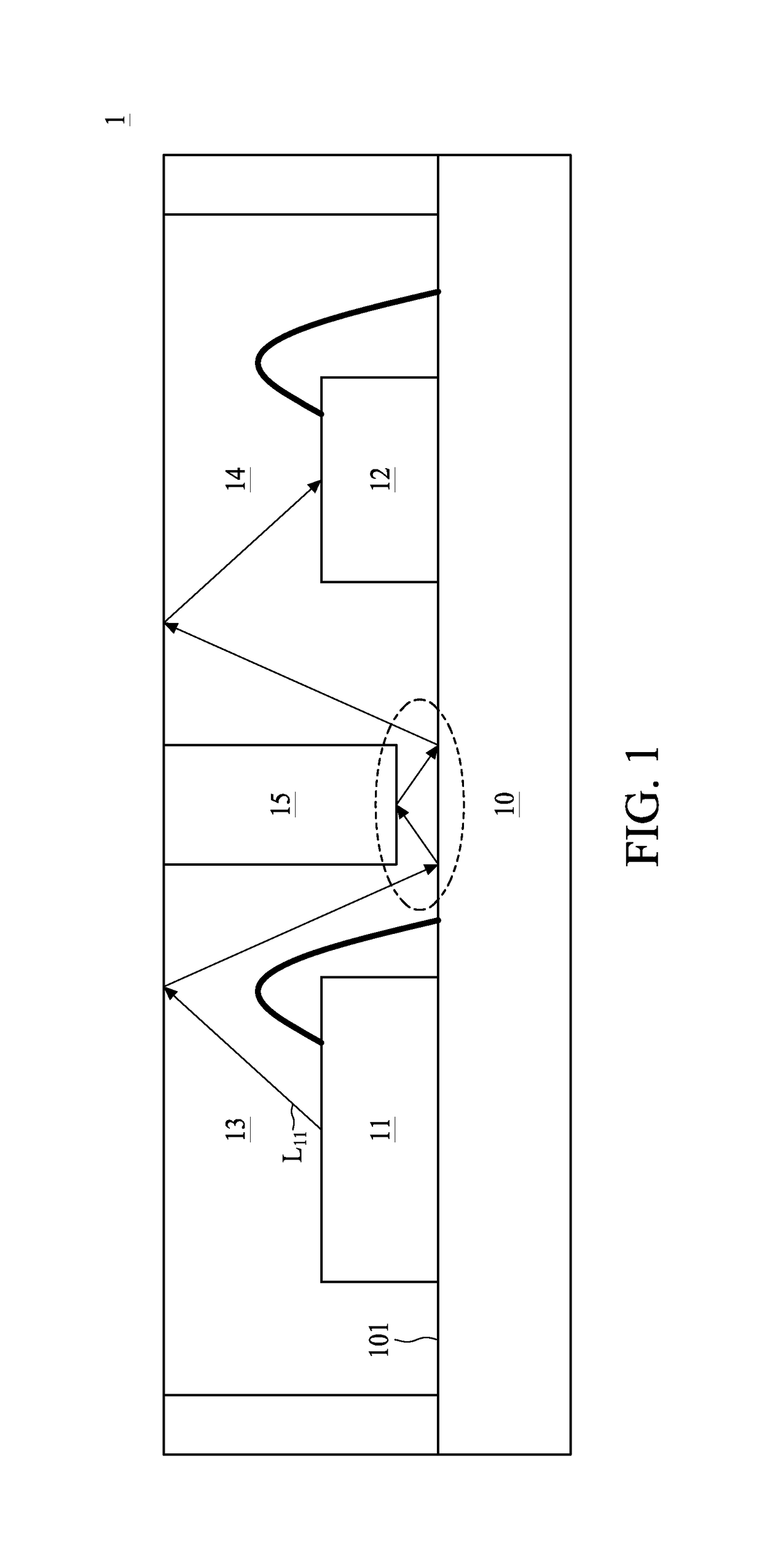
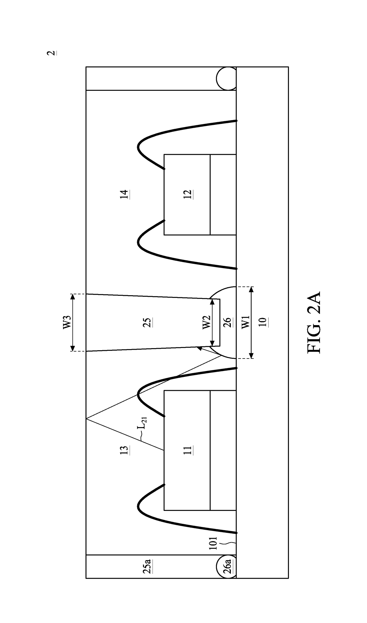
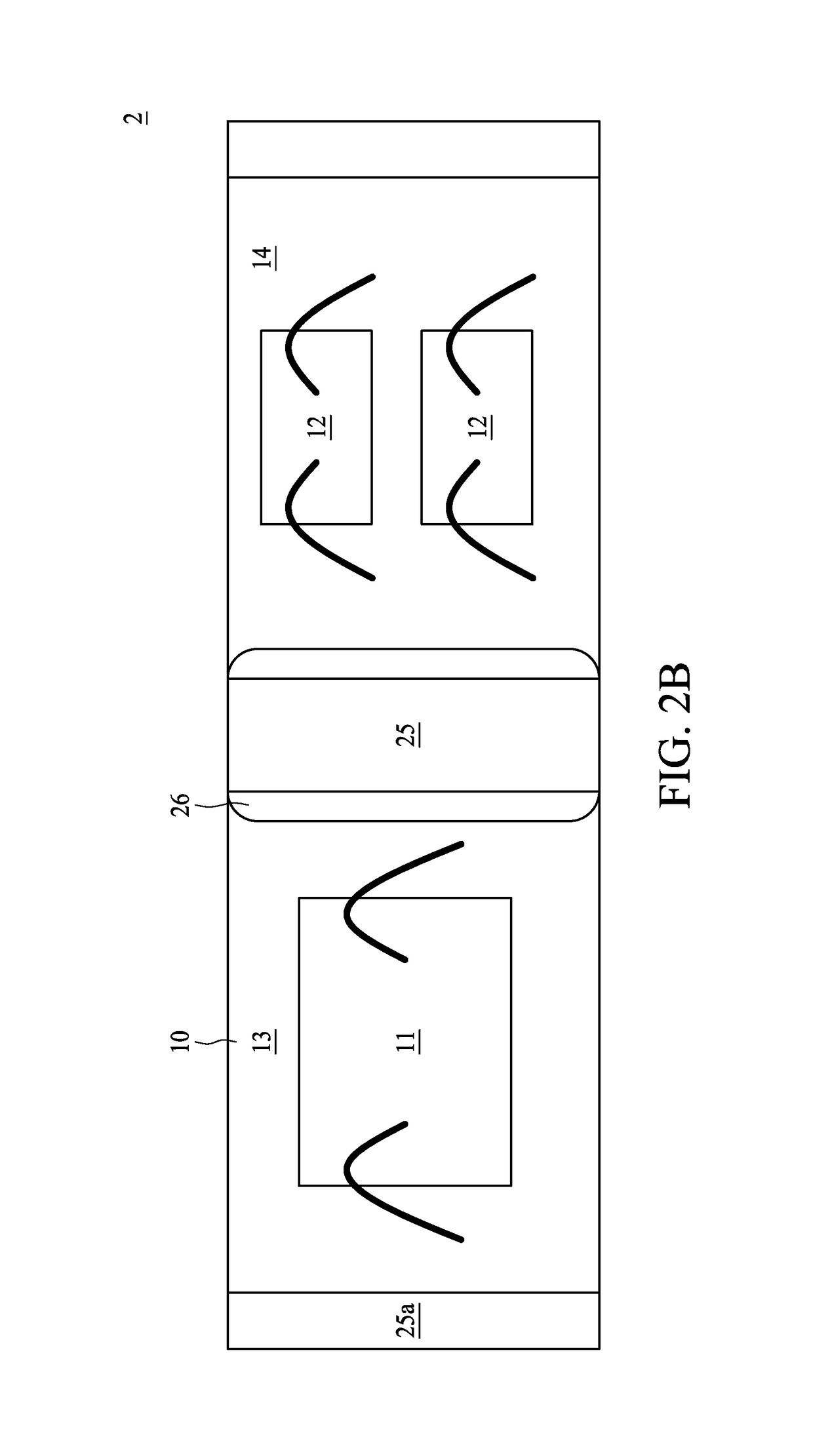
[0016]FIG. 1 illustrates a cross-sectional view of a semiconductor package device 1 in accordance with some embodiments of the present disclosure. The semiconductor package device 1 includes a carrier 10, electronic components 11, 12, package bodies 13, 14 and a wall structure 15.

[0017]The carrier 10 may include, for example, a substrate, a printed circuit board, such as a paper-based copper foil laminate, a composite copper foil laminate, or a polymer-impregnated glass-fiber-based copper foil laminate. The carrier 10 may include an interconnection structure, such as a conductive trace or a redistribution layer (RDL) and a dielectric layer such as prepreg layer or a polyimide layer.

[0018]The electronic component 11 is disposed on a top surface 101 of the carrier 10. In some embodiments, the electronic component 11 may be a light emitter or a light emitting device, such as an LED or other emitting die. For example, the electronic component 11 may include a light-emitting diode, a las...


PUM


Abstract

An optical device includes a carrier including a light transmitting layer and a light shielding layer disposed on the light transmitting layer. The optical device further includes a light emitter disposed on the carrier and a light detector disposed on the carrier. The optical device further includes a light transmitting encapsulant encapsulating the light emitter and the light detector, and a light shielding wall disposed in the light transmitting encapsulant and in contact with the light transmitting encapsulant and the light shielding layer.

Description

BACKGROUND1. Technical Field[0001]The present disclosure relates to a semiconductor package device, and more particularly, to a semiconductor package device including light emitting components.2. Description of the Related Art[0002]Light Emitting Diodes (LEDs), or laser diodes, are widely used for many applications. A semiconductor light emitting device can include an LED chip having one or more semiconductor layers. The layers can be configured to emit coherent and / or incoherent light when energized. During manufacture, a large number of LED semiconductor dies can be produced on a semiconductor wafer. The wafer can be probed and tested to accurately identify particular color characteristics of each die, such as color temperature. Then, the wafer can be singulated to cut the wafer into a plurality of LED chips. The LED chips can be packaged to provide external electrical connections, heat sinking, lenses or waveguides, environmental protection, and / or other features.[0003]An LED chi...

Claims


Application Information

Patent Timeline
Patent Type & Authority Patents(United States)
IPC IPC(8): H01L31/167H01L31/02H01L31/18H01L25/16H01L31/0216H01L33/54H01L33/62H01L33/44
CPCH01L31/167H01L25/167H01L31/02005H01L31/02164H01L33/44H01L33/54H01L33/62H01L31/1876H01L2933/0025H01L2933/005H01L23/552Y02P70/50
Inventor CHEN, PO-NIENCHIEN, YU-TINGLIN, YUEH-LUNGTSAI, TSUNG-YUEH
Owner ADVANCED SEMICON ENG INC
Features
  • R&D
  • Intellectual Property
  • Life Sciences
  • Materials
  • Tech Scout
  • Unparalleled Data Quality
  • Higher Quality Content
  • 60% Fewer Hallucinations
Learn More