Three-level power converter

a power converter and three-level technology, applied in the direction of dc-ac conversion without reversal, casings/cabinets/drawers, electrical equipment casings/cabinets/drawers, etc., can solve problems such as surge voltage, and achieve the effect of reducing wiring inductance, increasing device capacity, and inhibiting imbalanced current allotmen

Active Publication Date: 2018-12-11
FUJI ELECTRIC CO LTD
View PDF45 Cites 2 Cited by
  • Summary
  • Abstract
  • Description
  • Claims
  • Application Information

AI Technical Summary

Benefits of technology

[0033]According to the present invention, by forming separately the first module and the second module respectively housing a vertical arm and an intermediate arm forming a three-level inverter, optimum semiconductor switches can be applied to the modules in accordance with the specification of each device. In addition, due to the configuration in which the connecting terminal boards that extend from the respective modules are disposed close to and parallel to each other with insulating plates therebetween, wiring inductances of the DC circulating current paths of the three-level inverter can be minimized. In a case where the semiconductor switches are connected in parallel for the purpose of increasing the capacity of the device, the connecting terminal boards are simply extended commonly. Thus, not only is it possible to reduce the wiring inductances of the DC circulating current paths, but also the wiring inductances can be equalized, inhibiting imbalanced current allotment.

Problems solved by technology

Furthermore, in a circuit that uses semiconductor switching elements, typically a surge voltage occurs due to the current changing rate (di / dt) obtained at the time of a switching operation and a parasitic inductance on the circuit.
The surge voltage is a cause of overvoltage of a semiconductor switching element, which is often problematic.

Method used


Image

  • Three-level power converter
  • Three-level power converter
  • Three-level power converter

Examples


first embodiment

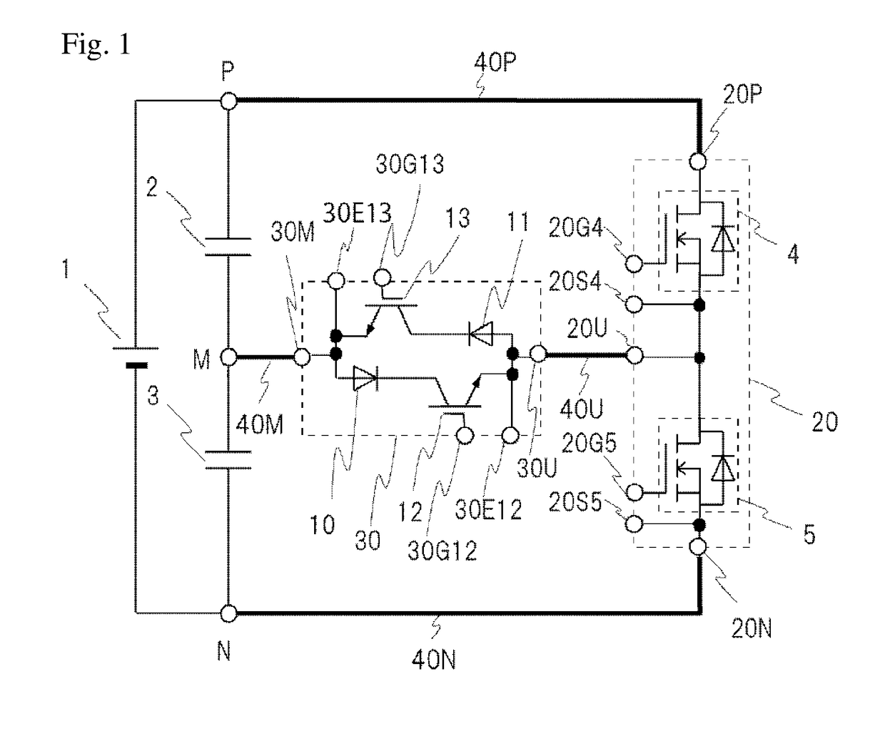
[0047]FIG. 1 is a circuit configuration diagram showing a single phase of a three-level inverter according to a first embodiment of the present invention.

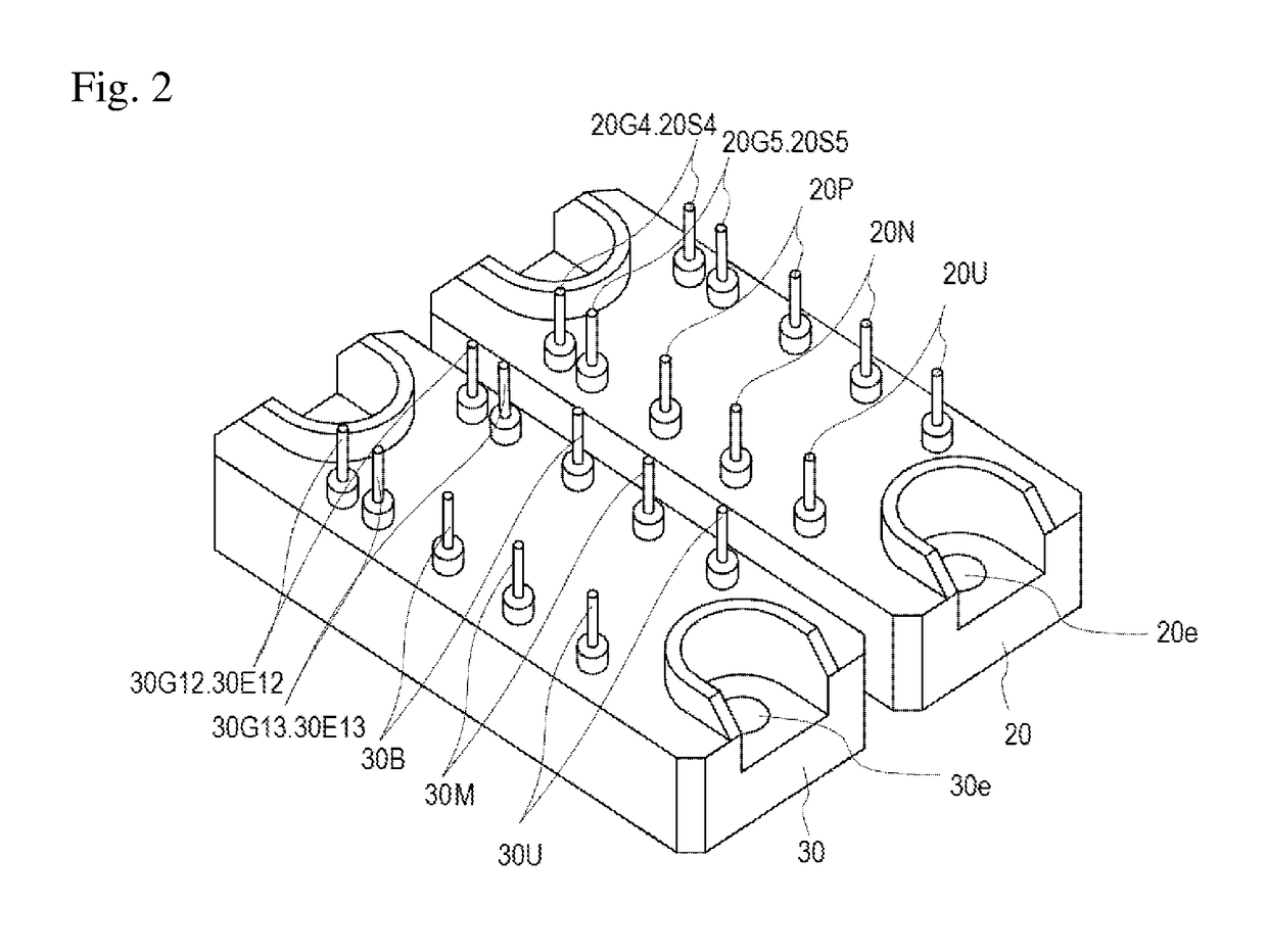
[0048]As shown in FIG. 1, a first module 20 houses a circuit that forms a vertical arm of a three-level inverter, in which semiconductor switches 4 and 5 configured with MOSFETs are connected in series. A bidirectional switch functioning as an intermediate arm of the three-level inverter is configured with diodes 10, 11 and IGBTs 12, 13, which are housed in a second module 30. The semiconductor switches applied to the vertical arm and the intermediate arm are not limited to the example shown in FIG. 1, and therefore various semiconductor switches such as high-speed switching elements made from wide band-gap semiconductor materials such as SiC (silicon carbide) can be used in accordance with the specifications of the devices used. Wide band-gap semiconductor materials have recently been put into practical use.

[0049]A high-potential ...

second embodiment

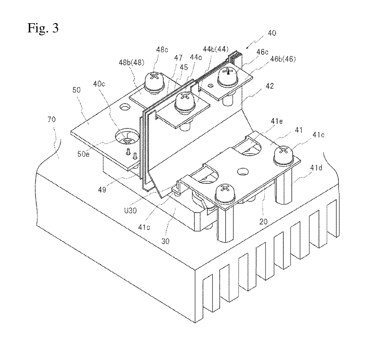
[0092]FIG. 9 shows a second embodiment of the present invention. In this example, the module 20 housing the vertical arm and the module 30 housing the intermediate arm are connected in two pairs and in parallel. FIG. 9 shows a simplified configuration of a connecting terminal board assembly without the insulating plates of the foregoing connecting terminal board assembly.

[0093]As shown in FIG. 9, two modules 20-1, 20-2 each housing a vertical arm and two modules 30-1, 30-2 each housing an intermediate arm are arranged alternately and in parallel.

[0094]These two pairs of modules that are disposed in parallel are provided with the connecting terminal boards 44A, 46A and 48A and the gate circuit board 50A, which are disposed across these two pairs of modules 20-1, 20-2 and 30-1, 30-2.

[0095]The high-potential connecting terminal board 48A is provided with two terminal connectors (48a-1, 48a-2) connected to the connecting terminals of the modules 20-1 and 20-2 each housing a vertical arm...

third embodiment

[0101]FIG. 10 shows a third embodiment of the present invention. In this example, the module housing the vertical arm and the module housing the intermediate arm are connected in three pairs in parallel. FIG. 10 shows a simplified configuration of a connecting terminal board assembly without the insulating plates of the foregoing connecting terminal board assembly, as with the second embodiment.

[0102]As shown in FIG. 10, three modules 20-1, 20-2, 20-3 each housing a vertical arm and three modules 30-1, 30-2, 30-3 each housing an intermediate arm are arranged alternately and in parallel.

[0103]These three pairs of modules that are disposed in parallel are provided with the connecting terminal boards 44B, 46B and 48B and a gate circuit board 50B, which are disposed across the six modules 20-1, 20-2, 20-3, 30-1, 30-2, and 30-3.

[0104]The high-potential connecting terminal board 48B is provided with three terminal connectors (48a-1, 48a-2, 48a-3) that are connected to the connecting termi...


PUM


Abstract

A three-level power converter includes a first module housing a vertical arm forming a three-level power conversion circuit; a second module disposed adjacent to the first module and housing an intermediate arm forming the three-level power conversion circuit; high-potential and low-potential connecting terminal boards each extending vertically, and having a lower end connected to connecting terminals on an upper surface of the first module, and an upper end provided with an external connecting end; and a flat intermediate-potential connecting terminal board extending vertically, and having a lower end connected to connecting terminals on an upper surface of the second module, and an upper end provided with an external connecting end. The high-potential, low-potential, and intermediate-potential connecting terminal boards are stacked close to and parallel to one another. Each of the external connecting ends is connected to a corresponding terminal of a DC capacitor.

Description

CROSS-REFERENCE TO RELATED APPLICATION[0001]This is a continuation application of PCT International Application No. PCT / JP2015 / 061544 filed on Apr. 15, 2015, which claims a priority of Japanese Patent Application No. 2014-171698 filed on Aug. 26, 2014.TECHNICAL FIELD[0002]The present invention relates to a three-level power converter that uses a semiconductor switch module, and more particularly to the wiring structures of a capacitor and a module.BACKGROUND ART[0003]A typical circuit of one phase of a three-level single-phase inverter or multi-phase inverter has the configuration shown in FIG. 11 of the present application. The inverter here means a circuit for converting a DC power into an AC power but also obviously converts an AC power into a DC power.[0004]In FIG. 11, reference numeral 1 represents a DC power source, the voltage of which is divided by capacitors 2, 3 to form three potentials, P, M and N. Reference numerals 4 to 7 each represent a semiconductor switching element...

Claims


Application Information

Patent Timeline
Patent Type & Authority Patents(United States)
IPC IPC(8): H02M7/537H02M7/00H02M7/48H02M7/483H05K5/02H01L25/11H05K5/00H02M7/487H01L25/18
CPCH02M7/003H01L25/115H01L25/18H02M7/48H02M7/537H05K5/0065H05K5/0247H02M7/483H02M7/487
Inventor MARUYAMA, KOJITANAKA, TAKAAKI
Owner FUJI ELECTRIC CO LTD
Why Eureka
Try Eureka